Diodes SDA006 User Manual

/
/
/
Please click here to visit our online spice models database.
DATA BUS TRANSIENT SUPPRESSOR / 3-PHASE FULL WAVE BRIDGE RECTIFIER
Features
• Fast Switching Speed
• Ultra-Small Surface Mount Package
• For 3-Phase Full Wave Bridge Rectification, or 3 Dataline Rail
Clamp
• Lead Free By Design/RoHS Compliant (Note 3)
• "Green" Device (Note 4)
IEC Compatibility (Note 5)
• 61000-4-2 (ESD) Air-10kV Contact-8kV
• 61000-4-5 (Surge) 8x20μs, 14.5 Amperes
Maximum Ratings @T
= 25°C unless otherwise specified
A
Characteristic Symbol Value Unit
Non-Repetitive Peak Reverse Voltage
Peak Repetitive Reverse Voltage
Working Peak Reverse Voltage
DC Blocking Voltage
RMS Reverse Voltage
Forward Continuous Current (Note 1)
Non-Repetitive Peak Forward Surge Current @ t = 1.0μs
@ t = 1.0ms
@ t = 1.0s
Clamping Voltage (Note 6) @ Ipp = 14.5A
8x20μs Waveform
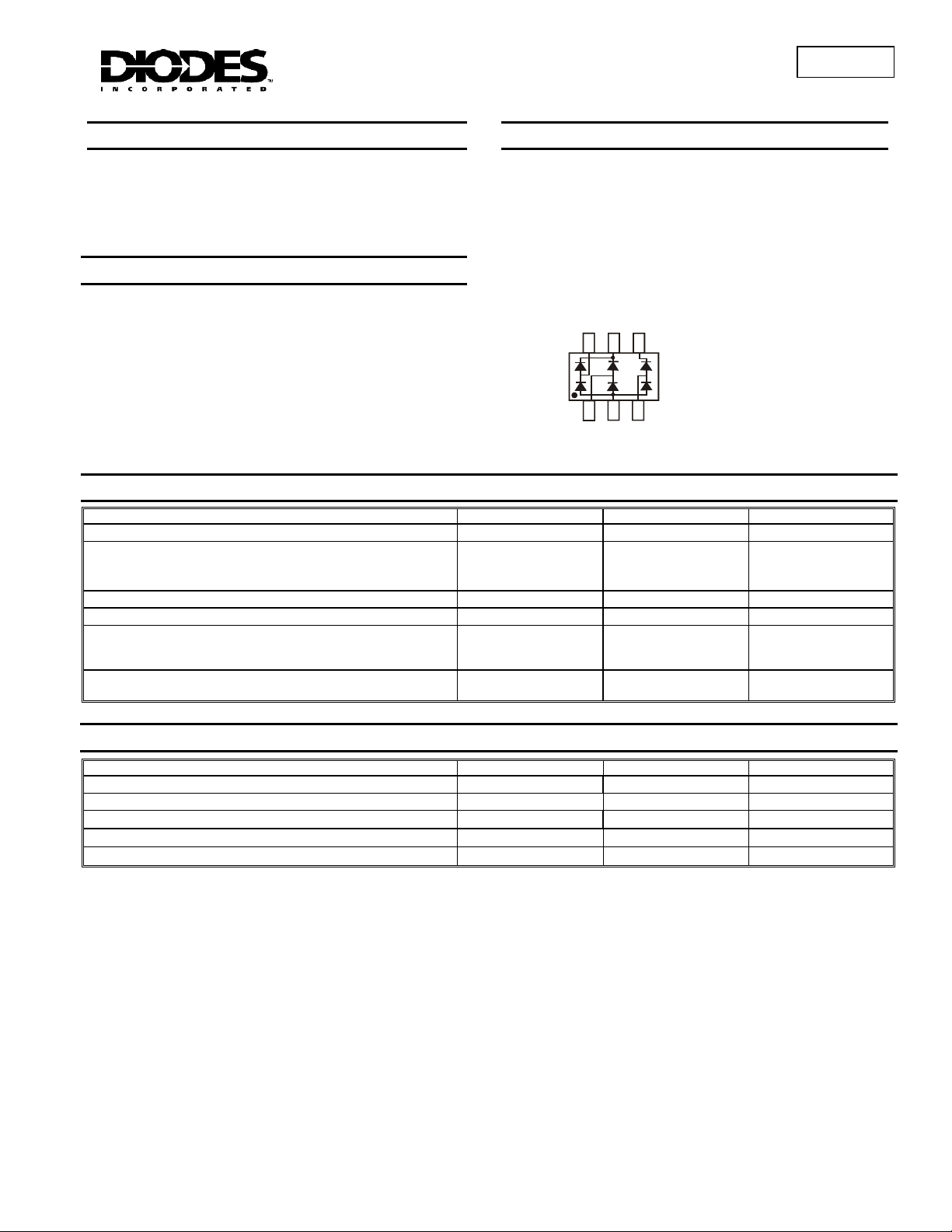
TOP VIEW
Mechanical Data
• Case: SOT-363
• Case Material: Molded Plastic, "Green" Molding Compound.
UL Flammability Classification Rating 94V-0 (Note 4)
• Moisture Sensitivity: Level 1 per J-STD-020D
• Terminals: Finish ⎯ Matte Tin annealed over Alloy 42
Leadframe. Solderable per MIL-STD-202, Method 208
• Marking Information: See Page 3
• Ordering Information: See Page 3
• Weight: 0.006 grams (approximate)
DC
3
+
V
3
CC
GND
1
/
/
DC-
1
TOP VIEW
DC
+
V
CC
DL
2
/
AC
2
100 V
75 V
53 V
215 mA
2.0
1.0
0.5
16 V
SOT-363
VRM
V
V
RWM
VR
V
R(RMS)
IFM
I
FSM
V
RRM
C
Internal Schematic
AC
DL
DL
AC
SDA006
A
Thermal Characteristics
Characteristic Symbol Value Unit
Power Dissipation (Note 1)
Power Dissipation (Note 2)
Thermal Resistance Junction to Ambient Air (Note 1)
Thermal Resistance Junction to Ambient Air (Note 2)
Operating and Storage Temperature Range
Notes: 1. Device mounted on FR-4 PCB, 1 inch x 0.85 inch x 0.062 inch; pad layout as shown on Diodes Inc. suggested pad layout document AP02001, which
SDA006
Document number: DS30559 Rev. 6 - 2
can be found on our website at http://www.diodes.com/datasheets/ap02001.pdf.
2. Device mounted on Alumina PCB, 0.4 inch x 0.3 inch x 0.024 inch; pad layout as shown on Diodes Inc. suggested pad layout document AP02001, which
can be found on our website at http://www.diodes.com/datasheets/ap02001.pdf.
3. No purposefully added lead.
4. Diodes Inc.'s "Green" policy can be found on our website at http://www.diodes.com/products/lead_free/index.php.
5. Tested with V
6. Reference to V
connected to Ground to simulate appropriate VCC decoupling to Ground.
CC
or Ground.
CC
PD
PD
R
JA
θ
R
JA
θ
TJ , T
STG
1 of 4
www.diodes.com
200 mW
300 mW
625
417
-65 to +150
°C/W
°C/W
°C
April 2008
© Diodes Incorporated

P, P
OWER
PATIO
TANT
O
US FORWARD CUR
RENT
T
T
O
US R
R
CUR
RENT
C
TOT
C
PACITANC
F
Electrical Characteristics @T
= 25°C unless otherwise specified
A
Characteristic
Reverse Breakdown Voltage (Note 7)
Forward Voltage (Note 7)
Reverse Current (Note 7)
Junction Capacitance (per element)
Capacitance, Between I/O Lines (I/O1 & I/O2)
Capacitance, Between I/O Line and Ground
Reverse Recovery Time
Notes: 7. Short duration pulse test used to minimize self-heating effect.
300
250
SDA006
Symbol Min Typ Max Unit Test Condition
V
(BR)R
VF
IR
75
⎯ ⎯
⎯ ⎯
CJ ⎯ ⎯
C
⎯
LL
C
⎯
LG
trr ⎯ ⎯
1
(A)
⎯ ⎯
0.715
0.855
1.0
1.25
2.5
50
30
25
2.0 pF
35
⎯
11
⎯
4.0 ns
V
IR = 2.5μA
IF = 1.0mA
IF = 10mA
V
IF = 50mA
IF = 150mA
VR = 75V
μA
VR = 75V, TJ = 150°C
μA
μA
VR = 25V, TJ = 150°C
nA
VR = 20V
VR = 0V, f = 1.0MHz
pF
VR = 0V, f = 1.0MHz
pF
VR = 0V, f = 1.0MHz
IF = IR = 10mA,
I
= 0.1 x IR, RL = 100Ω
rr
N (mW)
200
0.1
150
DISSI
100
0.01
ANE
D
50
F
I , INS
0.001
0
V , INSTANTANEOUS FORWARD VOLTAGE (V)
F
1.00.5
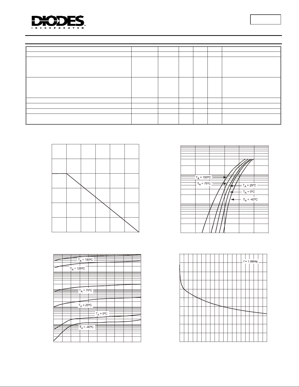
Fig. 2 Typical Forward Characteristics, Per Element
2.0
1.8
)
1.6
E (p
1.4
1.2
1.0
A
0.8
AL
0.6
,
T
0.4
1.5
10,000
(nA)
1,000
SE
EVE
ANE
AN
0
250 50 75 100 125 150
T , AMBIENT TEMPERATURE ( C)
A
Fig. 1 Power Derating Curve, Total Package
100
10
1
°
0.2
R
I, INS
0.1
0
Fig. 3 Typical Reverse Characteristics, Per Element
20 40 60 80 100
V , INSTANTANEOUS REVERSE VOLT AGE (V)
R
0.0
0
10
V , DC REVERSE VOLTAGE (V)
R
20
Fig. 4 Total Capac itance vs. Reverse Voltage ,
Per Element
30
40
SDA006
Document number: DS30559 Rev. 6 - 2
2 of 4
www.diodes.com
April 2008
© Diodes Incorporated
 Loading...