Diodes SD830, SD860 User Manual

Product Summary @T
V
(V) IO (A) V
RRM
30, 40, 60 8 0.7 100
= +25°C
A
FMAX
(V) I
RMAX
(μA)
Pb
SD830 –SD860
8.0A SCHOTTKY BARRIER RECTIFIERS
Features and Benefits
High Current Capability and Low Forward Voltage Drop
High Surge Capacity
Guard Ring for Transient Protection
Low Power Loss, High Efficiency
Lead Free Finish, RoHS Compliant (Note 1 & 2)
Description and Applications
8.0 A Schottky Barrier Rectifier in DO-201AD package, offers high
current capability and low forward voltage drop, designed with Guard
Ring for Transient Protection and high surge capacity.
Maximum Ratings (@T
Single phase, half wave, 60Hz, resistive or inductive load.
For capacitance load, derate current by 20%.
Peak Repetitive Reverse Voltage
Working Peak Reverse Voltage
DC Blocking Voltage
RMS Reverse Voltage
Average Rectified Output Current (See Figure 1)
Non-Repetitive Peak Forward Surge Current 8.3ms
Single Half Sine-Wave Superimposed on Rated Load
= +25°C, unless otherwise specified.)
A
Characteristic Symbol SD830 SD840 SD860 Unit
Mechanical Data
Case: DO-201AD
Case Material: Molded Plastic. UL Flammability Classification
Rating 94V-0
Moisture Sensitivity: Level 1 per J-STD-020C
Terminals: Finish - Bright Tin. Solderable per MIL-STD-202,
Method 208
Polarity: Cathode band
Mounting Position: Any
Weight: 1.1 grams (approximate)
V
VR
V
V
I
RRM
RWM
RM
(RMS)
I
O
FSM
30 40 60 V
21 28 42 V
8 A
175 A
Thermal Characteristics
Characteristic Symbol Value Unit
Typical Thermal Resistance Junction to Lead (Note 3) TA = +25°C R
Operating and Storage Temperature Range
T
J, TSTG
θJL
30 °C/W
-65 to +150 °C
Electrical Characteristics (@T
Characteristic Symbol Min Typ Max Unit Test Condition
Forward Voltage Drop
Leakage Current
Typical Junction Capacitance (Note 4)
Notes: 1. EU Directive 2002/95/EC (RoHS) & 2011/65/EU (RoHS 2) compliant. All applicable RoHS exempltions applied.
2. See http://www.diodes.com/quality/lead_free.html
and Lead-free.
3. Thermal resistance from junction to lead vertical PC board mounting, 9.5mm lead length.
4. Measured at 1.0MHz and applied reverse voltage of 4.0V.
SD830 – SD860
Document number: DS23006 Rev. 7 - 2
= +25°C, unless otherwise specified.)
A
V
F
I
R
C
J
– 0.55 0.7 V
– –
– 550 – pF
for more information about Diodes Incorporated’s definitions of Halogen- and Antimony-free, “Green”
1 of 3
www.diodes.com
IF = 8A, TJ = +25°C
= V
R
R
= V
RRM
RRM
, TJ = +25°C
, TJ = +100°C
September 2013
© Diodes Incorporated
1.0
50
mA
mA
V
V
VR = 4V, f=1.0 MHz

R
GE REC
TIF
CUR
RENT
TANT
O
US FORWARD CUR
RENT
C, CAPACITANC
F
P
O
RWAR
D SURGE CUR
REN
T
10
(A)
8
6
IED
50
(A)
10
SD830 –SD860
4
A
2
O
I, AVE
0
20 40 60 80 100 120 140
T , LEAD TEMPERATURE (ºC)
L
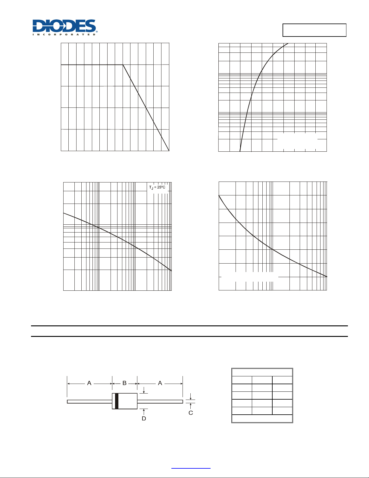
Fig. 1 Forward Current Derating Curve
ANE
I, INS
F
0.1
1.0
0.1
4,000
f = 1MHz
)
E (p
1,000
j
100
0.1
1.0
V , REVERSE VOLTAGE (VOLTS)
R
Fig. 3 Typical Junction Capacitance
10
100
200
(A)
175
150
125
100
75
50
EAK F
25
FSM
I,
0
1.0 10 100
Fig. 4 Max Non-Repetitive Peak Fwd Surge Current
Package Outline Dimensions
Please see AP02002 at http://www.diodes.com/datasheets/ap02002.pdf for latest version.
TJ = 25ºC
Pulse Width = 300ms
1% Duty Cycle
0.3 0.5
V , INSTANTANEOUS FWD VOLTAGE (V)
F
Fig. 2 Typical Forward Characteristics
8.3 ms Single Half Sine-Wave
NUMBER OF CYCLES AT 60Hz
DO-201AD
Dim Min Max
A 25.40 -
B 7.20 9.50
C 1.20 1.30
D 4.80 5.30
All Dimensions in mm
0.7
0.9 1.1
SD830 – SD860
Document number: DS23006 Rev. 7 - 2
2 of 3
www.diodes.com
September 2013
© Diodes Incorporated
 Loading...