DIODES SD101AW, SD101CW, SD101BW Datasheet

Features
Low Forward Voltage Drop
·
Guard Ring Construction for
·
Transient Protection
Negligible Reverse Recovery Time
·
Very Low Reverse Capacitance
·
Mechanical Data
Case: SOD-123, Plastic
·
Case material - UL Flammability Rating
·
Classification 94V-0
Moisture sensitivity: Level 1 perJ-STD-020A
·
Polarity: Cathode Band
·
Leads: Solderable per MIL-STD-202,
·
Method 208
Marking: Date Code & Type Code, See Page 2
·
Type Codes: SD101AW S1 or SK
·
· Weight: 0.01 grams (approx.)
· Ordering Information: See Page 2
Maximum Ratings
SD101BW S2 or SK
SD101CW S3 or SK
@ TA= 25°C unless otherwise specified
SD101AW - SD101CW
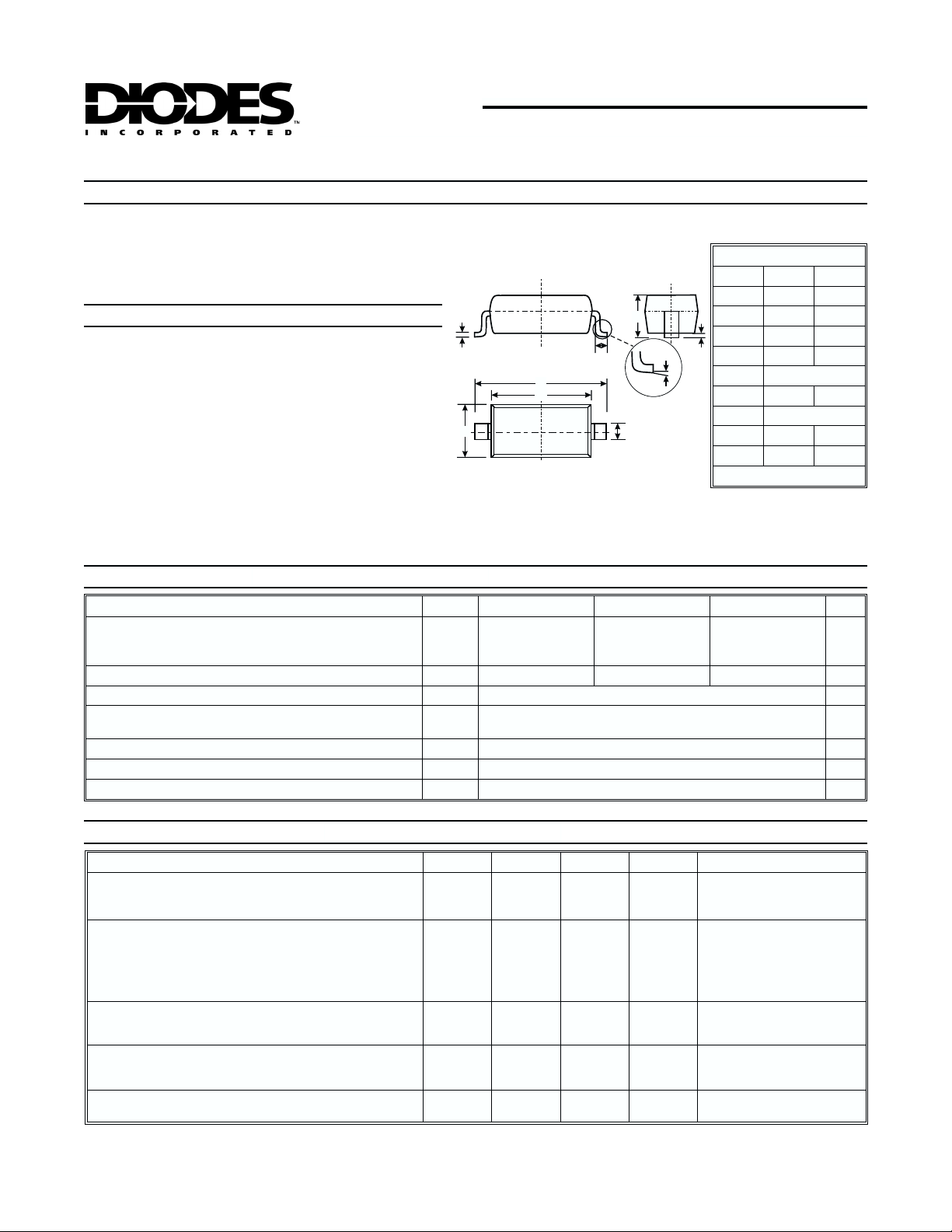
SCHOTTKY BARRIER SWITCHING DIODE
SOD-123
Dim Min Max
A 3.55 3.85
H
A
B
C
D
G
a
E
B 2.55 2.85
J
C 1.40 1.70
D — 1.35
E 0.55 Typical
G0.25—
H 0.11 Typical
J — 0.10
a 0° 8°
All Dimensions in mm
Characteristic Symbol SD101AW SD101BW SD101CW Unit
Peak Repetitive Reverse Voltage
Working Peak Reverse Voltage
DC Blocking Voltage
RMS Reverse Voltage
Forward Continuous Current (Note 1)
Non-Repetitive Peak Forward Surge Current @ t £ 1.0s
Power Dissipation (Note 1)
Thermal Resistance, Junction to Ambient Air (Note 1)
Operating and Storage Temperature Range
Electrical Characteristics
Characteristic Symbol Min Max Unit Test Condition
Reverse Breakdown Voltage (Note 2) SD101AW
Forward Voltage Drop (Note 2) SD101AW
Peak Reverse Current (Note 2) SD101AW
Total Capacitance SD101AW
Reverse Recovery Time
Notes: 1. Part mounted on FR-4 board with recommended pad layout, which can be found on ourwebsite
at http://www.diodes.com/datasheets/ap02001.pdf.
2. Short duration test pulse used to minimize self-heating effect.
@ t = 10ms
@ TA= 25°C unless otherwise specified
SD101BW
SD101CW
SD101BW
SD101CW
SD101AW
SD101BW
SD101CW
SD101BW
SD101CW
SD101BW
SD101CW
V
RRM
V
RWM
V
V
R(RMS)
I
FM
I
FSM
P
R
qJA
T
j,TSTG
V
V
R
d
(BR)R
FM
I
RM
C
T
t
rr
60 50 40
42 35 28
15
50
2.0
400 mW
300
-65 to +125 °C
= 10mA
60
50
40
¾
¾ 200 nA
¾
¾ 1.0 ns
¾ V
0.41
0.40
0.39
1.00
0.95
0.90
2.0
2.1
2.2
pF
I
R
= 10mA
I
R
= 10mA
I
R
= 1.0mA
I
F
I
= 1.0mA
F
I
= 1.0mA
V
F
I
= 15mA
F
I
= 15mA
F
I
= 15mA
F
= 50V
V
R
V
= 40V
R
V
= 30V
R
= 0V, f = 1.0MHz
V
R
= IR= 5.0mA,
I
F
= 0.1 x IR,RL= 100W
I
rr
V
V
mA
mA
A
°C/W
DS11012 Rev. 9 - 2 1 of 2 SD101AW-SD101CW

00
d
g
10
g
2
P , POWER DISSIPATION (mW)
5
400
300
200
100
F
I , FORWARD CURRENT (mA)
1.0
0.1
A
B
C
0
025
50
T , AMBIENT TEMPERATURE (°C)
A
Fi
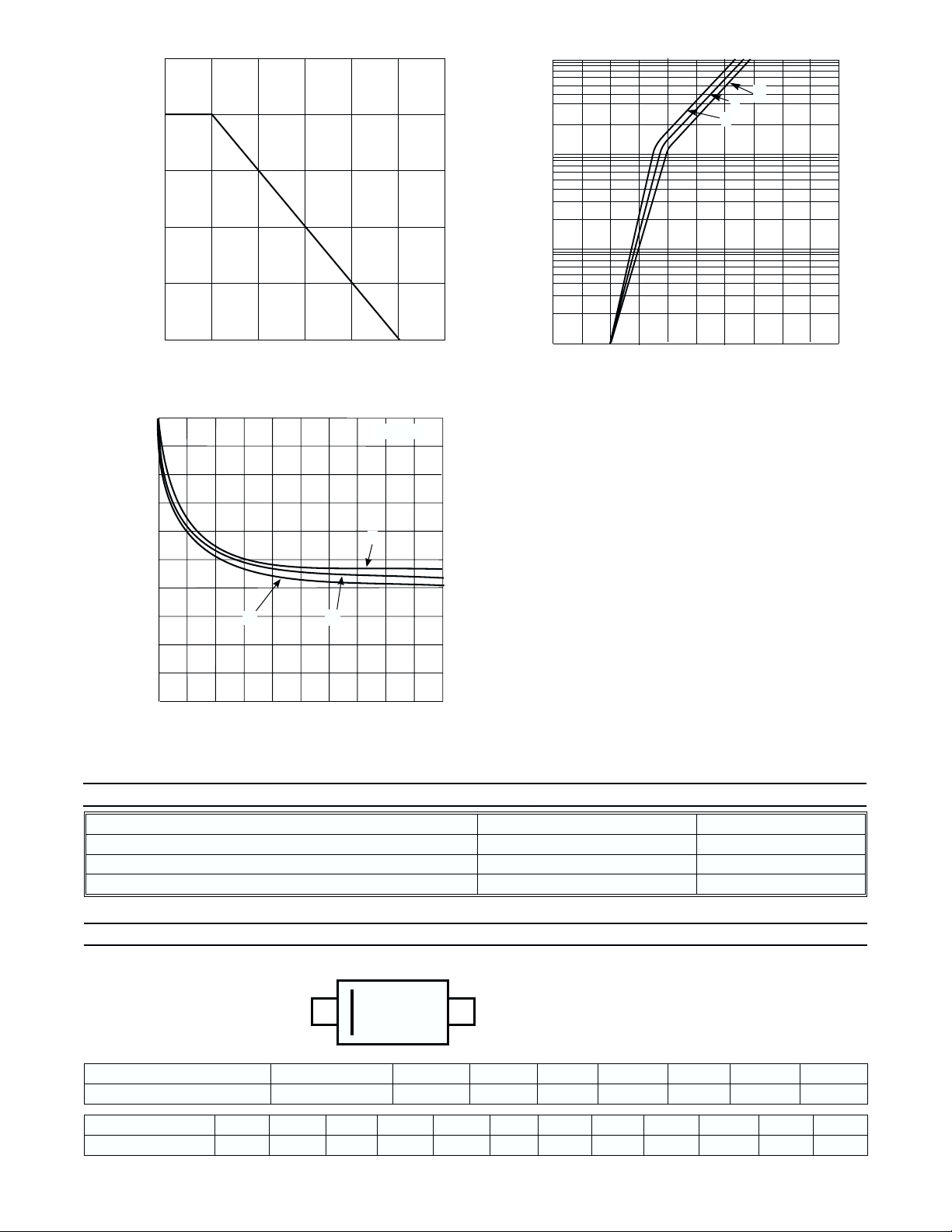
.1 Power DeratingCurve
75
100
125 150
T = 25 Cj°
C
1
B
T
C , TOTAL CAPACITANCE (pF)
A
0
01020304050
V , REVERSE VOLTAGE (V)
R
Fig.3 Typ. Total Capacitance vs Reverse Voltage
0.01
0 0.5 1.0
V , FORWARD VOLTAGE (V)
F
Fi
.2Typical Forward Characteristic
Ordering Information
Note: 3. For Packaging Details, go to our website at http://www.diodes.com/datasheets/ap02007.pdf.
(Note 3)
Device Packaging Shipping
SD101AW-7
SD101BW-7
SD101CW-7
SOD-123
SOD-123
SOD-123
3000/Tape and Reel
3000/Tape and Reel
3000/Tape and Reel
Marking Information
XX = Product Type Marking Code
YM = Date Code Marking
XX
Date Code Key
Year 1998 1999 2000 2001
Code JKLM
Month Jan Feb March Apr May Jun Jul
Code 1234567
YM
DS11012 Rev. 9 - 2 2 of 2 SD101AW-SD101CW
Y = Year (ex: N = 2002)
M = Month (ex: 9 = September)
2002 2003 2004 2005
NPR S
Aug Sep Oct Nov Dec
89 O ND
 Loading...