Diodes SBR3A40SA User Manual

Features
Low Leakage Current
Patented Super Barrier Rectifier Technology
Soft, Fast Switching Capability
+150°C Operating Junction Temperature
Lead Free Finish, RoHS Compliant (Notes 1 & 2)
Halogen and Antimony Free. “Green” Device (Note 3)
SBR3A40SAQ Qualified to AEC-Q101 standards for High
Reliability.
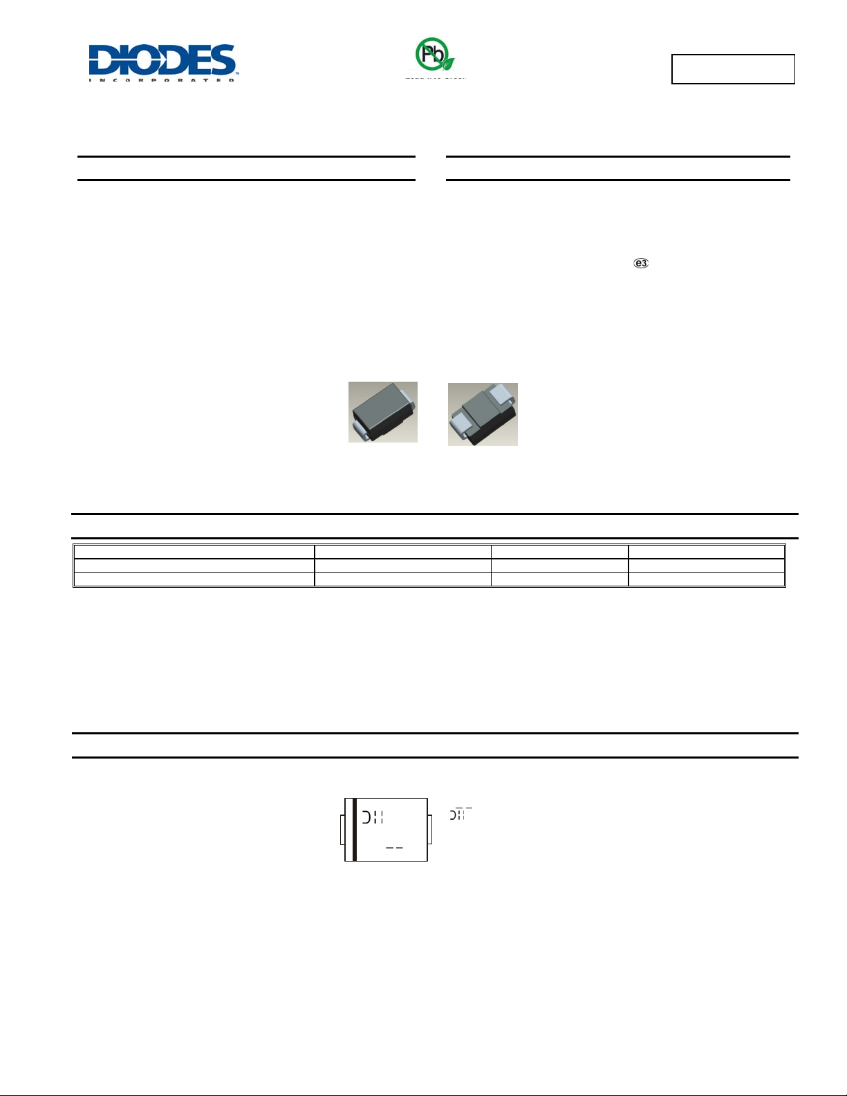
Top View Bottom View
Green
SBR3A40SA
3.0A SBR
®
SUPER BARRIER RECTIFIER
SMA
Mechanical Data
Case: SMA
Case Material: Molded Plastic, “Green” Molding compound.
UL Flammability Classification Rating 94V-0
Moisture Sensitivity: Level 1 per J-STD-020D
Terminals: Lead Free Plating (Matte Tin Finish.) Solderable
per MIL-STD-202, Method 208
Polarity Indicator: Cathode Band
Marking Information: See Page 3
Ordering Information: See Page 3
Weight: 0.064 grams (approximate)
Ordering Information (Note 4)
Part Number Compliance Case Packaging
SBR3A40SA-13 Commercial SMA 5000/Tape & Reel
SBR3A40SAQ-13 Automotive SMA 5000/Tape & Reel
Notes: 1. EU Directive 2002/95/EC (RoHS) & 2011/65/EU (RoHS 2) compliant. All applicable RoHS exemptions applied.
2. See http://www.diodes.com/quality/lead_free.html for more information about Diodes Incorporated’s definitions of Halogen- and Antimony-free, "Green"
and Lead-free.
3. Halogen- and Antimony-free "Green” products are defined as those which contain <900ppm bromine, <900ppm chlorine (<1500ppm total Br + Cl) and
<1000ppm antimony compounds.
4. For packaging details, go to our website at http://www.diodes.com/products/packages.html.
5. Product manufactured with Data Code 0924 (week 24, 2009) and newer are built with Green Molding Compound.
Marking Information
Notes: 6. Device has a cathode band (as shown above) and may also have a cathode notch.
SBR is a registered trademark of Diodes Incorporated.
SBR3A40SA
Document number: DS31107 Rev. 11 - 2
YWW
S V4
www.diodes.com
SV 4 = Product Type Marking Code
= Manufacturers’ code marking
YWW = Date Code Marking
Y = Last digit of year (ex: 7 for 2007)
WW = Week code 01 to 52
XX
1 of 5
September 2013
© Diodes Incorporated

)
(BR)
SBR3A40SA
Maximum Ratings (@T
= +25°C, unless otherwise specified.)
A
Single phase, half wave, 60Hz, resistive or inductive load
For capacitance load, derate current by 20%.
Characteristic Symbol Value Unit
V
Peak Repetitive Reverse Voltage
Working Peak Reverse Voltage
DC Blocking Voltage
Maximum Voltage Rate of Change (Rated VR)
RMS Reverse Voltage
Average Rectified Output Current
Non-Repetitive Peak Forward Surge Current 8.3ms
Single Half Sine-Wave Superimposed on Rated Load
V
RRM
RWM
V
RM
40 V
dv/dt 10,000 V/μs
V
R(RMS
I
I
O
FSM
28 V
3 A
45 A
Thermal Characteristics
Maximum Thermal Resistance
Thermal Resistance Junction to Soldering (Note 7)
Thermal Resistance Junction to Ambient (Note 8)
Thermal Resistance Junction to Case (Note 8)
Power Dissipation (Note 8) @TA = +25°C PD 1.2 W
Operating and Storage Temperature Range
Characteristic Symbol Value Unit
R
JS
R
JA
R
JC
T
, T
J
STG
5
124
°C/W
14.3
-65 to +150 °C
Electrical Characteristics (@T
= +25°C, unless otherwise specified.)
A
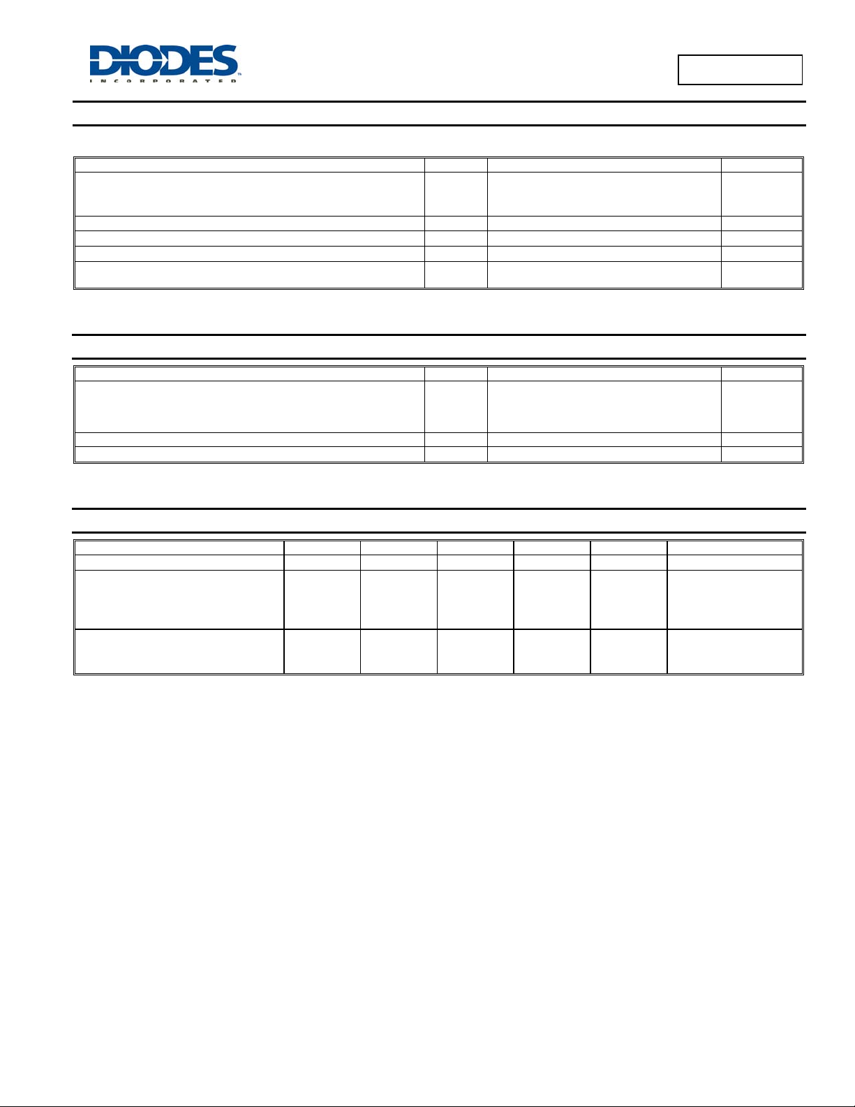
Characteristic Symbol Min Typ Max Unit Test Condition
Reverse Breakdown Voltage (Note 10)
Forward Voltage Drop
Leakage Current (Note 10)
Notes: 7. Theoretical R
8. FR-4 PCB, 2 oz. Copper, minimum recommended pad layout per http://www.diodes.com/datasheets/ap02001.pdf.
9. Polymide PCB, 2 oz. Copper, minimum recommended pad layout per http://www.diodes.com/datasheets/ap02001.pdf.
10. Short duration pulse test used to minimize self-heating effect.
11. FR-4 PCB, 2 oz. Copper, single side 16 x MRP, 1” x 1” PC Board.
calculated from the top center of the die straight down to the PCB cathode tab solder junction.
JS
V
R
V
F
I
R
40 – – V
–
–
–
0.30
0.33
0.43
–
45
–
80
9
0.35
0.38
0.50
0.48
250
400
40
V
μA
μA
mA
IR = 0.4mA
I
= 0.5A, TJ = +25°C
F
= 1.0A, TJ = +25°C
I
F
I
= 3.0A, TJ = +25°C
F
= 3.0A, TJ = +125°C
I
F
V
= 5V, TJ = +25°C
R
V
= 40V, TJ = +25°C
R
= 40V, TJ = +125°C
V
R
SBR is a registered trademark of Diodes Incorporated.
SBR3A40SA
Document number: DS31107 Rev. 11 - 2
2 of 5
www.diodes.com
September 2013
© Diodes Incorporated
 Loading...