Diodes SBR2A40P1 User Manual

)
θ
Features
• Low Forward Voltage Drop
• Low Leakage Current
• Superior Reverse Avalanche Capability
• Excellent High Temperature Stability
• Patented Interlocking Clip Design for High Surge Current
Capacity
• Patented Super Barrier Rectifier Technology
• Soft, Fast Switching Capability
• 150ºC Operating Junction Temperature
• ±16KV ESD Protection (HBM, 3B)
• ±25KV ESD Protection (IEC61000-4-2 Level 4, Air Discharge)
• Lead Free Finish, RoHS Compliant (Note 1)
• “Green” Molding Compound (No Br, Sb)
• Qualified to AEC-Q 101 Standards for High Reliability
SBR2A40P1
SURFACE MOUNT SUPER BARRIER RECTIFIER
Mechanical Data
• Case: PowerDI®123
• Case Material: Molded Plastic, “Green” Molding Compound.
UL Flammability Classification Rating 94V-0
• Moisture Sensitivity: Level 1 per J-STD-020
• Polarity Indicator: Cathode Band
• Terminals: Finish - Matte Tin annealed over Copper leadframe.
Solderable per MIL-STD-202, Method 208
• Marking Information: See Page 4
• Ordering Information: See Page 4
• Weight: 0.018 grams (approximate)
Top View
2.0A SBR
PowerDI
®
123
®
Maximum Ratings @T
= 25°C unless otherwise specified
A
Single phase, half wave, 60Hz, resistive or inductive load.
For capacitance load, derate current by 20%.
Characteristic Symbol Value Unit
V
Peak Repetitive Reverse Voltage
Working Peak Reverse Voltage
DC Blocking Voltage
RMS Reverse Voltage
Average Rectified Output Current (See Figure 1)
Non-Repetitive Peak Forward Surge Current 8.3ms
Single Half Sine-Wave Superimposed on Rated Load
Repetitive Peak Avalanche Power (1μs, 25°C)
V
V
R(RMS
P
RRM
RWM
V
I
FSM
ARM
I
RM
O
40 V
28 V
2.0 A
50 A
6,000 W
Thermal Characteristics
Characteristic Symbol Value Unit
Maximum Thermal Resistance
Thermal Resistance Junction to Soldering (Note 2)
Thermal Resistance Junction to Ambient (Note 3)
Thermal Resistance Junction to Ambient (Note 4)
Operating and Storage Temperature Range
Notes: 1. EU Directive 2002/95/EC (RoHS). All applicable RoHS exemptions applied, see EU Directive 2002/95/EC Annex Notes.
2. Theoretical R
3. FR-4 PCB, 2 oz. Copper, minimum recommended pad layout per http://www.diodes.com/datasheets/ap02001.pdf.
4. Polymide PCB, 2 oz. Copper, minimum recommended pad layout per http://www.diodes.com/datasheets/ap02001.pdf.
calculated from the top center of the die straight down to the PCB cathode tab solder junction.
θJS
SBR and PowerDI are registered trademarks of Diodes Incorporated.
SBR2A40P1
Document number: DS30919 Rev. 10 - 2
www.diodes.com
R
R
R
T
, T
J
1 of 5
JS
θ
JA
θ
JA
STG
5
180
ºC/W
115
-65 to +150 ºC
April 2010
© Diodes Incorporated

(BR)
P, P
OWER
PATIO
Electrical Characteristics @T
= 25°C unless otherwise specified
A
Characteristic Symbol Min Typ Max Unit Test Condition
Reverse Breakdown Voltage (Note 5)
V
R
40 - - V
- 0.265 0.315
- 0.38 0.43
Forward Voltage Drop
V
F
- 0.45 0.50
- 0.17 0.22
- 0.325 0.375
- 0.42 0.47
- 8 40 µA
Leakage Current (Note 5)
I
R
- 16 100 µA
- 1.3 8 mA
- 2.1 10 mA
Notes: 5. Short duration pulse test used to minimize self-heating effect.
2
1.5
N (W)
10,000
1,000
100
T =150 C
A
T =100 C
°
SBR2A40P1
IR = 100µA
I
= 0.1A, TJ = 25ºC
F
= 1.0A, TJ = 25ºC
I
F
= 2.0A, TJ = 25ºC
I
V
°
A
T= -65C
A
F
= 0.1A, TJ = 125ºC
I
F
= 1.0A, TJ = 125ºC
I
F
= 2.0A, TJ = 125ºC
I
F
= 5V, TJ = 25ºC
V
R
= 40V, TJ = 25ºC
V
R
= 5V, TJ = 125ºC
V
R
= 40V, TJ = 125ºC
V
R
°
1
DISSI
T=25C
°
A
10
0.5
D
1
F
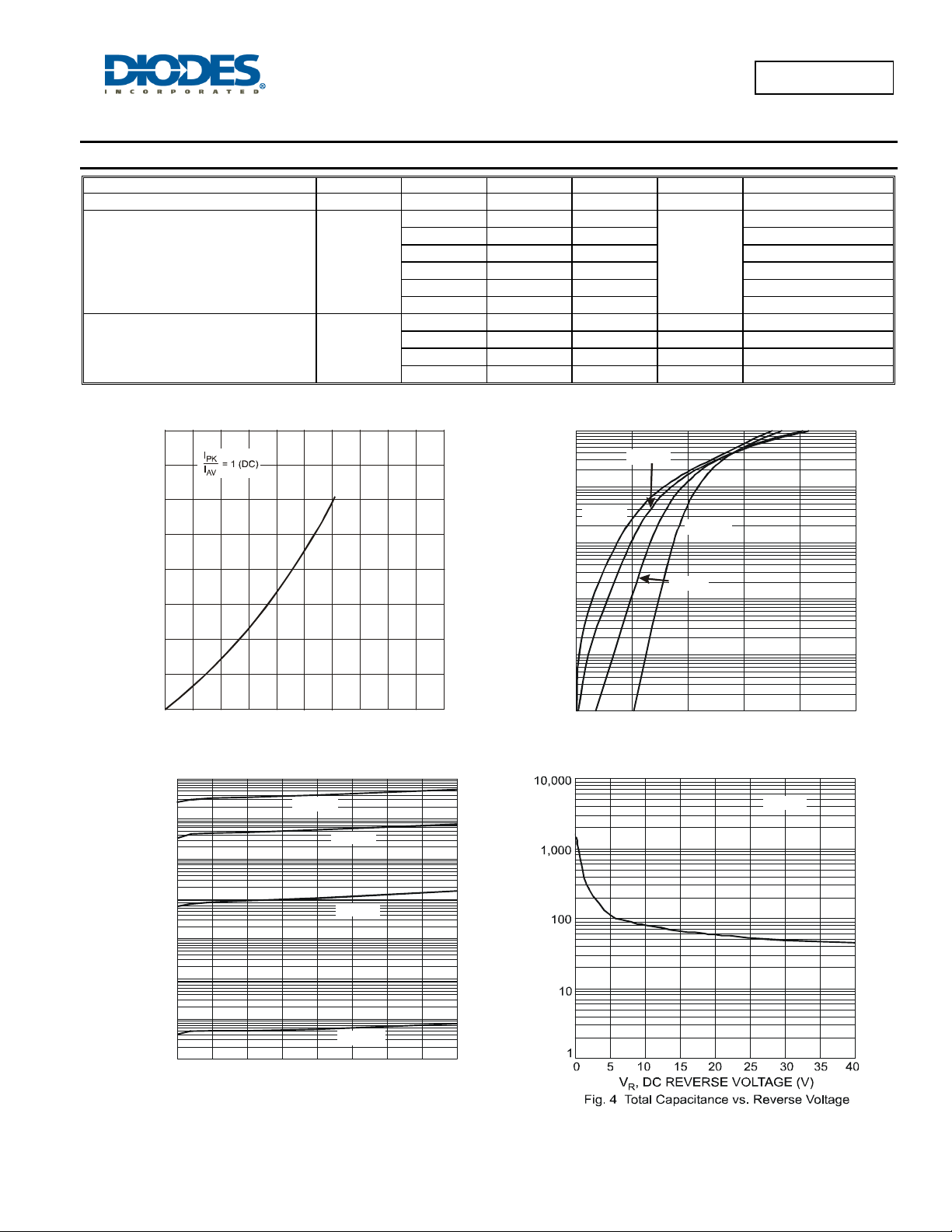
I , INSTANTANEOUS FORWARD CURRENT (mA)
0.1
0 0.2 0.4 0.6 0.8 1
V , INSTANTANEOUS FORWARD VOLTAGE (V)
F
Fig. 2 Typical Forward Characteristics
f = 1MHZ
10,000
μ
0
0
123
I , AVERAGE FORWARD CURRENT (A)
F(AV)
Fig. 1 Forward Power Dissipation
T =150 C
°
A
4
5
1,000
T =100 C
°
A
100
10
T=25C
°
A
1
0.1
T
C , TOTAL CAPACITANCE (pF)
0.01
T= -65C
°
R
I , INSTANTANENOUS LEAKAGE CURRENT ( A)
0.001
010203040
V , INSTANTANEOUS REVERSE VOLTAGE (V)
R
Fig. 3 Typical Reverse Characteristics
A
SBR and PowerDI are registered trademarks of Diodes Incorporated.
SBR2A40P1
Document number: DS30919 Rev. 10 - 2
2 of 5
www.diodes.com
April 2010
© Diodes Incorporated
 Loading...