Diodes SBR12A45SD1 User Manual

A
Features
• Designed as Bypass Diodes for Solar Panels
• Selectively Rated for +200°C Maximum Junction Temperature
for High Thermal Reliability
• Patented Super Barrier Rectifier Technology
• High Forward Surge Capability
• Ultra Low Forward Voltage Drop
• Excellent High Temperature Stability
• Lead-Free Finish; RoHS Compliant (Notes 1 & 2)
• Halogen and Antimony Free. “Green” Device (Note 3)
SBR12A45SD1
SUPER BARRIER RECTIFIER
Mechanical Data
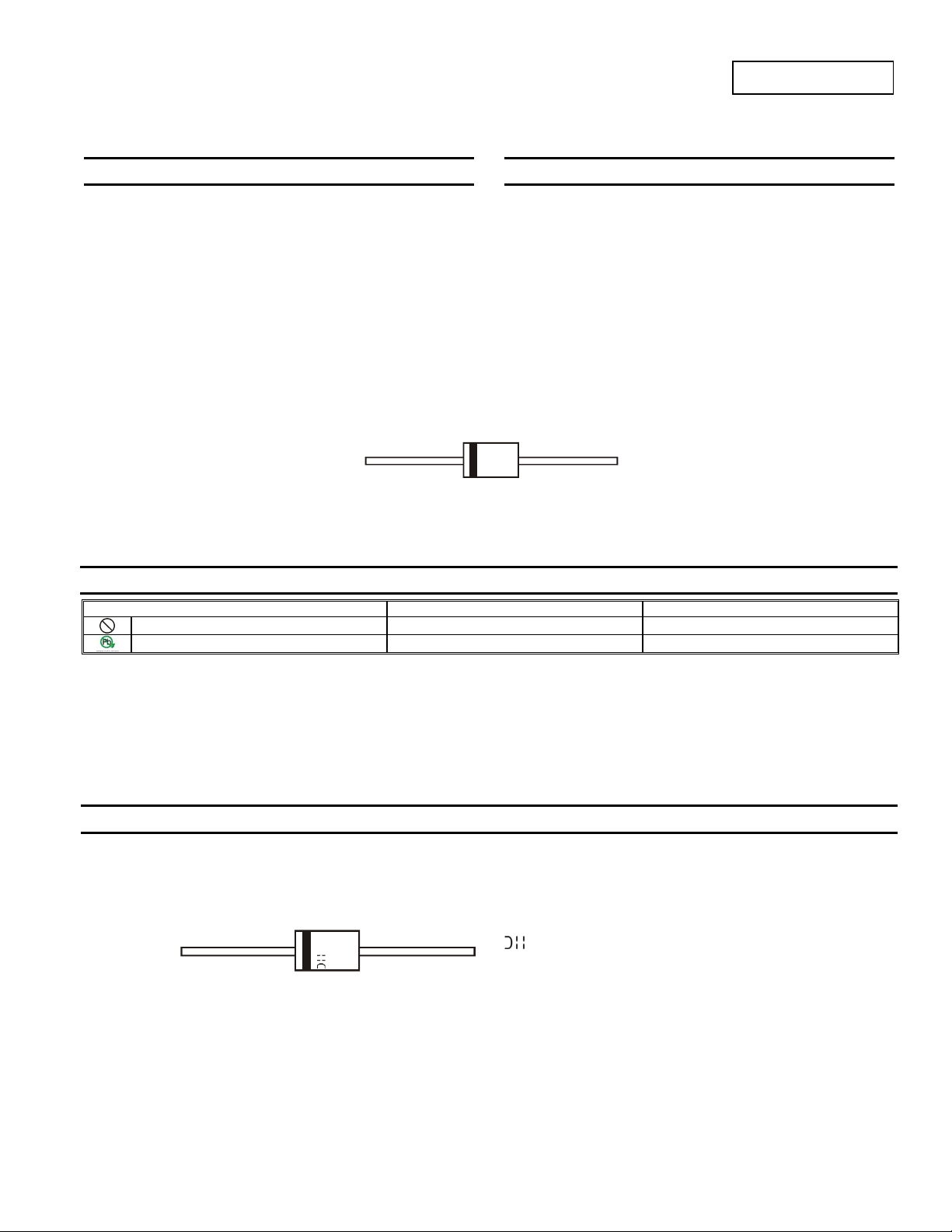
• Case: DO-201AD
• Case Material: Molded Plastic, UL Flammability Classification
Rating 94V-0
• Moisture Sensitivity: Level 1 per J-STD-020
• Terminals: Finish – Tin Plated Leads. Solderable per MIL-STD-
202, Method 208
• Weight: 1.21 grams (approximate)
Top View
12A SBR
®
Ordering Information (Notes 4 & 5)
Pb
Green
Notes: 1. EU Directive 2002/95/EC (RoHS) & 2011/65/EU (RoHS 2) compliant. All applicable RoHS exemptions applied.
2. See http://www.diodes.com for more information about Diodes Incorporated’s definitions of Halogen- and Antimony-free, "Green" and Lead-free.
5. For Green Molding version, add ‘–G’ to part number (ex. SBR12A45SD1-T-G)
3. Halogen- and Antimony-free "Green” products are defined as those which contain <900ppm bromine, <900ppm chlorine (<1500ppm total Br + Cl) and
<1000ppm antimony compounds.
4. For packaging details, go to our website at http://www.diodes.com.
Part Number Case Packaging
SBR12A45SD1-T DO-201AD 1200/Tape & Reel, 13-inch
SBR12A45SD1-T-G DO-201AD 1200/Tape & Reel, 13-inch
Marking Information
AB
YWW
SBR12A45
SBR12A45SD1
Document number: DS31452 Rev. 6 - 2
SBR is a registered trademark of Diodes Incorporated.
www.diodes.com
SBR12A45 = Product Type Marking Code
B = Foundry and Assembly Code
= Manufacturers’ code marking
YWW = Date Code Marking
Y = Last digit of year (ex: 8 for 2008)
WW = Week code (01 to 53)
1 of 4
July 2012
© Diodes Incorporated

)
θ
(BR)
Maximum Ratings (@T
= +25°C, unless otherwise specified.)
A
Single phase, half wave, 60Hz, resistive or inductive load.
For capacitance load, derate current by 20%.
Characteristic Symbol Value Unit
Peak Repetitive Reverse Voltage
Working Peak Reverse Voltage
DC Blocking Voltage
RMS Reverse Voltage
Average Rectified Output Current
Non-Repetitive Avalanche Energy
= +25°C , IAS = 20A , L = 8.5mH)
(T
J
Non-Repetitive Peak Forward Surge Current 8.3ms
Single Half Sine-Wave Superimposed on Rated Load
Peak Repetitive Reverse Surge Current (2µS – 1KHz)
Thermal Characteristics
Characteristic Symbol Value Unit
Typical Thermal Resistance
Thermal Resistance Junction to Ambient (Note 6)
Thermal Resistance Junction to Lead (Note 6) T
Operating Temperature Range
Storage Temperature Range
= +135°C
L
V
R
VR ≤ 50% V
DC Forward Mode ≤200
≤ 80% V
RRM
RRM
SBR12A45SD1
V
RRM
V
RWM
V
RM
V
R(RMS
I
O
AS 20 mJ
E
I
FSM
I
RRM
R
JA
θ
R
JL
TJ
T
STG
45 V
32 V
12 A
200 A
2 A
31
°C/W
7.2
-65 to +150
≤180
°C
-65 to +175 °C
Electrical Characteristics (@T
= +25°C, unless otherwise specified.)
A
Characteristic Symbol Min Typ Max Unit Test Condition
Reverse Breakdown Voltage (Note 7)
Forward Voltage Drop
Leakage Current (Note 7)
Notes: 6. Device mounted on 2" x 2" (50mm x 50mm) copper pad, with lead length 0.5".
7. Short duration pulse test used to minimize self-heating effect.
V
V
F
I
R
45 — — V
R
—
—
—
—
—
—
0.43
0.40
50
—
27
0.48
0.44
500
40
100
V
μA
mA
mA
IR = 0.5mA
= 12A, TJ = +25°C
I
F
= 12A, TJ = +125°C
I
F
V
= 45V, TJ = +25°C
R
= 45V, TJ = +125°C
V
R
V
= 45V, TJ = +150°C
R
SBR12A45SD1
Document number: DS31452 Rev. 6 - 2
SBR is a registered trademark of Diodes Incorporated.
2 of 4
www.diodes.com
July 2012
© Diodes Incorporated
 Loading...