

Page 1
θ
Please click here to visit our online spice models database.
Features
• Low Forward Voltage Drop
• Low Reverse Leakage
• Excellent High Temperature Stability
• Patented Super Barrier Rectifier Technology
• Soft, fast switching capability
• 150ºC Operating Junction Temperature
• Lead, Halogen and Antimony Free, RoHS Compliant
• “Green” Device (Note 1)
NEW PRODUCT
Maximum Ratings @T
Single phase, half wave, 60Hz, resistive or inductive load.
For capacitance load, derate current by 20%.
Peak Repetitive Reverse Voltage
Working Peak Reverse Voltage
DC Blocking Voltage
Average Rectified Output Current
Non-Repetitive Peak Forward Surge Current
8.3ms Single Half Sine-Wave Superimposed on Rated Load
= 25°C unless otherwise specified
A
Characteristic Symbol Value Unit
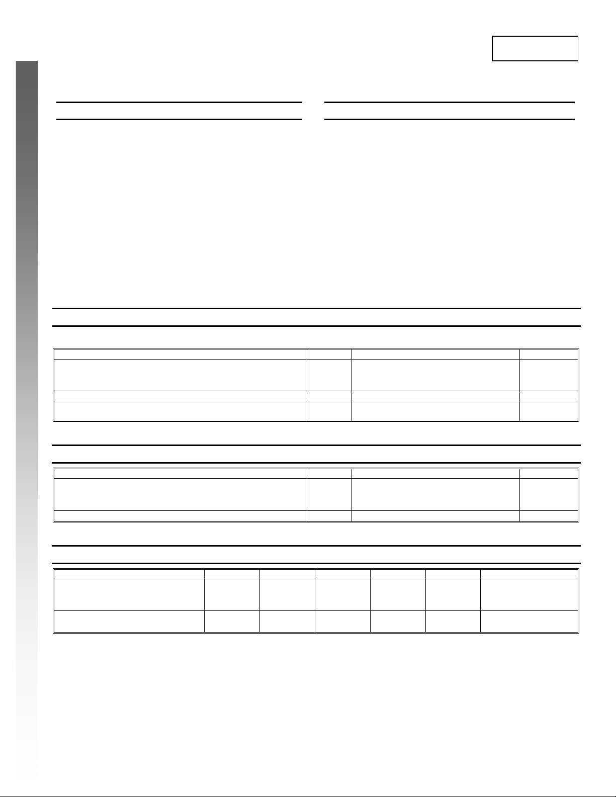
Mechanical Data
• Case: SOD-123
• Case Material: Molded Plastic, “Green” Molding Compound.
UL Flammability Classification Rating 94V-0
• Moisture Sensitivity: Level 1 per J-STD-020D
• Leads: Solderable per MIL-STD-202, Method 208
• Lead Free Plating (Matte Tin Finish annealed over Alloy 42
leadframe)
• Polarity: Cathode Band
• Marking Information: See Page 3
• Ordering Information: See Page 3
• Weight: 0.004 grams (approximate)
Top View
V
RRM
V
RWM
V
RM
I
O
I
FSM
SBR0560S1
0.5A SBR
®
SUPER BARRIER RECTIFIER
60 V
500 mA
15 A
Thermal Characteristics
Characteristic Symbol Value Unit
Typical Thermal Resistance
Thermal Resistance Junction to Ambient Air (Note 2)
Thermal Resistance Junction to Ambient Air (Note 3)
Operating and Storage Temperature Range
Electrical Characteristics @T
Characteristic Symbol Min Typ Max Unit Test Condition
Forward Voltage (Per Diode)
Leakage Current (Note 4)
Notes: 1. No purposefully added lead. Halogen and Antimony Free.
2. Part mounted on FR-4 board with recommended pad layout, which can be found on our website at http://www.diodes.com/datasheets/ap02001.pdf.
3. Part mounted on Polymide board with recommended pad layout, which can be found on our website at http://www.diodes.com/datasheets/ap02001.pdf.
SBR is a registered trademark of Diodes Incorporated.
SBR0560S1
Document number: DS31525 Rev. 2 - 2
4. Short duration pulse test used to minimize self-heating effect.
A
R
JA
θ
R
JA
, T
T
J
STG
= 25°C unless otherwise specified
V
F
I
R
-
-
1 of 4
www.diodes.com
-
0.44
-
-
-
305
271
-65 to +150 ºC
I
0.44
0.50
0.46
100
25
V
µA
mA
= 0.25A, TJ = 25ºC
F
I
= 0.5A, TJ = 25ºC
F
= 0.5A, TJ = 125ºC
I
F
V
= 60V, TJ = 25ºC
R
V
= 60V, TJ = 125ºC
R
ºC/W
June 2009
© Diodes Incorporated
Page 2
P
P
OWER
PAT
O
N
RAG
O
RWARD CUR
REN
T
T
N
T T
PER
TUR
C
NEW PRODUCT
0.5
10
SBR0560S1
0.45
0.4
1
(W)
I
DISSI
0.35
0.3
0.25
0.2
0.1
0.01
T = 150°C
A
T = 125°C
A
T = 85°C
A
T = 25°C
A
0.15
,
D
0.1
0.001
0.05
F
0
0 0.2 0.4 0.6 0.8 1
I , AVERAGE FORWARD CURRENT (A)
F(AV)
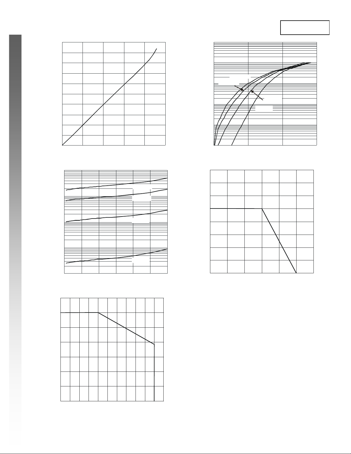
Fig. 1 Forward Power Dissipation
10,000
T = 150°C
1,000
T = 125°C
A
A
0.0001
I , INSTANT ANEOUS FORWARD CURRENT (A)
(A)
0 200 400 600
V , INSTANTANEOUS FORWARD VOL TAGE (mV)
F
Fig. 2 Typical Forwar d Characteristics
0.8
0.7
0.6
R
I , INSTANTANEOUS REVERSE CURRENT (µA)
T = 85°C
100
A
10
T = 25°C
A
1
0102030405060
V , INSTANTANEOUS REVERSE VOLTAGE (V)
R
Fig. 3 Typical Reverse Characteristics
175
150
)
E (°
125
A
100
EM
75
50
, AMBIE
A
25
0.5
0.4
E F
0.3
0.2
0.1
F(AV)
I, AVE
0
25 50 75 100 125 150 175
T , AMBIENT TEMPERATURE (°C)
A
Fig. 4 Forward Current Derating Curve
0
0 6 12 18 24 30 36 42 48 54 60
V , DC REVERSE VOLTAGE (V)
R
66
Fig. 5 Operating Temperature Derating
SBR is a registered trademark of Diodes Incorporated.
SBR0560S1
Document number: DS31525 Rev. 2 - 2
2 of 4
www.diodes.com
June 2009
© Diodes Incorporated
Page 3

Ordering Information (Note 5)
Part Number Case Packaging
SBR0560S1-7 SOD-123 3000/Tape & Reel
Notes: 5. For packaging details, go to our website at http://www.diodes.com/datasheets/ap02007.pdf.
Marking Information
NEW PRODUCT
56
YM
56 = Product Type Marking Code
Package Outline Dimensions
B
M
C
H
A
K
L
SOD-123
Dim Min Max
A 0.55 Typ
B 1.40 1.70
C 3.55 3.85
H 2.55 2.85
J 0.00 0.10
K 1.00 1.35
L 0.25 0.40
M 0.10 0.15
α
All Dimensions in mm
0 8°
SBR0560S1
Suggested Pad Layout
C
SBR is a registered trademark of Diodes Incorporated.
SBR0560S1
Document number: DS31525 Rev. 2 - 2
X
Y
G
Z
www.diodes.com
3 of 4
Dimensions Value (in mm)
Z 4.9
G 2.5
X 0.7
Y 1.2
C 3.7
June 2009
© Diodes Incorporated
Page 4

DIODES INCORPORATED MAKES NO WARRANTY OF ANY KIND, EXPRESS OR IMPLIED, WITH REGARDS TO THIS DOCUMENT,
INCLUDING, BUT NOT LIMITED TO, THE IMPLIED WARRANTIES OF MERCHANTABILITY AND FITNESS FOR A PARTICULAR PURPOSE
(AND THEIR EQUIVALENTS UNDER THE LAWS OF ANY JURISDICTION).
Diodes Incorporated and its subsidiaries reserve the right to make modifications, enhancements, improvements, corrections or other changes
without further notice to this document and any product described herein. Diodes Incorporated does not assume any liability arising out of the
application or use of this document or any product described herein; neither does Diodes Incorporated convey any license under its patent or
trademark rights, nor the rights of others. Any Customer or user of this document or products described herein in such applications shall assume
all risks of such use and will agree to hold Diodes Incorporated and all the companies whose products are represented on Diodes Incorporated
website, harmless against all damages.
Diodes Incorporated does not warrant or accept any liability whatsoever in respect of any products purchased through unauthorized sales channel.
Should Customers purchase or use Diodes Incorporated products for any unintended or unauthorize d application, Customers shall indemnify and
hold Diodes Incorporated and its representatives harmless against all claims, damages, expenses, and attorney fees arising out of, directly or
NEW PRODUCT
indirectly, any claim of personal injury or death associated with such unintended or unauthorized application.
Products described herein may be covered by one or more United States, international or foreign patents pending. Product names and markings
noted herein may also be covered by one or more United States, international or foreign trademarks.
Diodes Incorporated products are specifically not authorized for use as critical components in life support devices or systems without the express
written approval of the Chief Executive Officer of Diodes Incorporated. As used herein:
A. Life support devices or systems are devices or systems which:
1. are intended to implant into the body, or
labeling can be reasonably expected to result in significant injury to the user.
B. A critical component is any component in a life support device or system whose failure to perform can be reasonably expected to cause the
failure of the life support device or to affect its safety or effectiveness.
Customers represent that they have all necessary expertise in the safety and regulatory ramifications of their life support devices or systems, and
acknowledge and agree that they are solely responsible for all legal, regulatory and safety-related requirements concerning their products and any
use of Diodes Incorporated products in such safety-critical, life support devices or systems, notwithstanding any devices- or systems-related
information or support that may be provided by Diodes Incorporated. Further, Customers must fully indemnify Diodes Incorporated and its
representatives against any damages arising out of the use of Diodes Incorporated products in such safety-critical, life support devices or systems.
Copyright © 2009, Diodes Incorporated
www.diodes.com
2. support or sustain life and whose failure to perform when properly used in accordance with instructions for use provided in the
IMPORTANT NOTICE
LIFE SUPPORT
SBR0560S1
SBR is a registered trademark of Diodes Incorporated.
SBR0560S1
Document number: DS31525 Rev. 2 - 2
www.diodes.com
4 of 4
June 2009
© Diodes Incorporated
 Loading...