

Page 1
Features
• Low Leakage Current
• Patented Super Barrier Rectifier Technology
cellent High Temperature Stability
• Ex
• Soft, Fast Sw
• 150ºC Operating Junction Temperature
• Lead Free Finish, RoHS Compliant (Note 1)
Green” Molding Compound (No Br, Sb)
• “
• Qualified to A
NEW PRODUCT
Maximum Ratings @T
Single phase, half wave, 60Hz, resistive or inductive load.
For capacitance load, derate current by 20%.
Peak Repetitive Reverse Voltage
Working Peak Reverse Voltage
DC Blocking Voltage
RMS Reverse Voltage
Average Rectified Output Current (See Figure 1)
Non-Repetitive Peak Forward Surge Current 8.3ms
Single Half Sine-Wave Superimposed on Rated Load
itching Capability
EC-Q101 Standards for High Reliability
= 25°C unless otherwise specified
A
Characteristic Symbol Value Unit
Mechanical Data
• Case: DFN1006-2
Top View Bottom View
• Case Material: Molded Plastic, “Green” Molding Compound.
UL F
lammability Classification Rating 94V-0
• Moisture Sensitivity
• Polarity
Indicator: Cathode Dot
• Terminals: Finish - NiPdAu over Copper leadframe. Solderable
per MIL-STD-202, Method 208
• Marking Information: See Page 3
• Ordering Information: See Page 3
• Weight: 0.001 grams (approximate)
V
RRM
V
RWM
V
RM
V
R(RMS)
I
O
I
FSM
SBR0220LP
0.2A SBR
®
SUPER BARRIER RECTIFIER
: Level 1 per J-STD-020D
20 V
14 V
0.2 A
5.0 A
Thermal Characteristics
Maximum Thermal Resistance
Thermal Resistance Junction to Soldering (Note 2)
Thermal Resistance Junction to Ambient (Note 3)
Operating and Storage Temperature Range
Electrical Characteristics @T
Characteristic Symbol Min Typ Max Unit Test Condition
Reverse Breakdown Voltage (Note 4)
Forward Voltage Drop
Leakage Current (Note 4)
Notes: 1. RoHS revision 13.2.2003. High temperature solder exemption applied, see EU Directive Annex Note 7.
2. Theoretical R
3. FR-4 PCB, 2oz. Copper, minimum recommended pad layout per http://www.
4. Short duration pulse test used to minimize self-heating effect.
SBR is a registered trademark of Diodes Incorporated.
SBR0220LP
Document number: DS31062 Rev. 5 - 2
Characteristic Symbol Value Unit
R
JS
θ
R
JA
θ
T
, T
J
STG
= 25°C unless otherwise specified
A
V
(BR)R
V
F
I
R
calculated from the top center of the die straight down to the PCB cathode tab solder junction.
θJS
20 - - V
0.38
-
0.30
0.44
0.38
-
2
0.43
0.42
0.33
0.48
0.41
50
1.3
diodes.com/datasheets/ap02001.pdf.
1 of 3
www.diodes.com
17
304
ºC/W
-65 to +150 ºC
I
= 400µA
R
I
= 0.1A, TJ = 25ºC
F
I
= 0.1A, TJ = 150ºC
V
µA
mA
F
= 0.2A, TJ = 25ºC
I
F
I
= 0.2A, TJ = 150ºC
F
V
= 20V, TJ = 25ºC
R
= 20V, TJ = 150ºC
V
R
March 2008
© Diodes Incorporated
Page 2
P
P
OWER
P
TIO
0.4
0.3
N (W)
A
0.2
DISSI
,
D
0.1
NEW PRODUCT
0
0 0.1 0.2 0.3 0.4 0.5 0.6
I , AVERAGE FORWARD CURRENT (A)
F(AV)
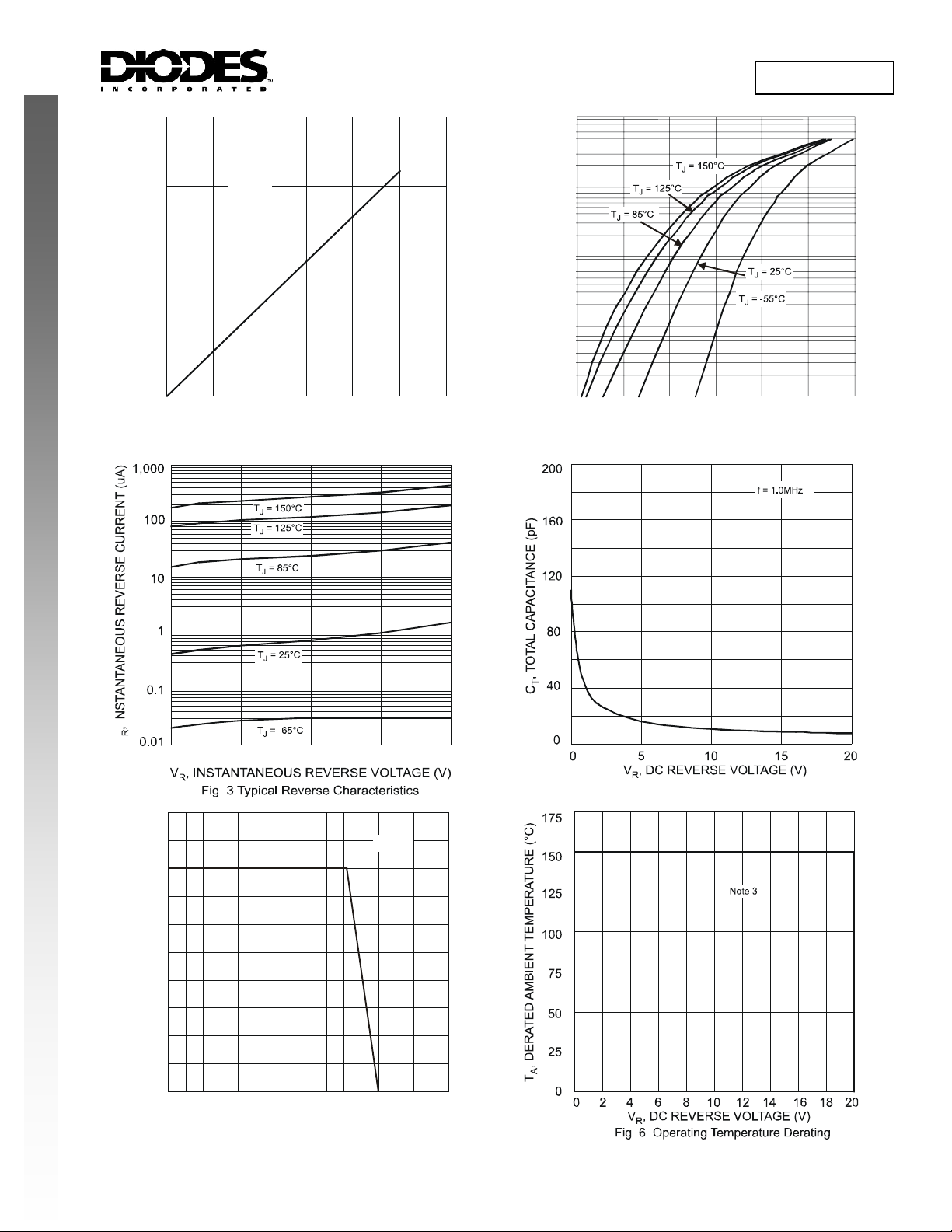
Fig. 1 Forward Power Dissipation
T =150°C
J
SBR0220LP
1,000
100
10
1
F
I , INSTANTANEOUS FORWARD CURRENT (mA)
0.1
0 0.2 0.4 0.6
V , INSTANTANE OUS FORWA RD VOLTAG E ( V)
F
Fig.2 Typical Forward Characteristics
0 5 10 15 20
Fig. 4 Total Capacitance vs. Reverse Voltage
0.25
Note 3
0.2
0.15
0.1
0.05
F(AV)
I , AVERAGE FORWARD CURRENT(A)
0
0 25 50 75 100 125 150
T , AMBIENT TEMPERA TURE (°C)
A
Fig. 5 Forward Current Derating Curve
BR is a registered trademark of Diodes Incorporated.
S
SBR0220LP
Document number: DS31062 Rev. 5 - 2
175 200
www.diodes.com
2 of 3
March 2008
© Diodes Incorporated
Page 3

Ordering Information (Note 5)
Part Number Case Packaging
SBR0220LP-7 DFN1006-2 3000/Tape & Reel
Notes: 5. For packaging details, go to our website at http://www.diodes.com/datasheets/ap02007.pdf.
Marking Information
Package Outline Dimensions
NEW PRODUCT
SBR0220LP
22 = Product Type Marking Code
22
G
H
A
B
D
R
N
Dot Denotes Cathode Side
C
DFN1006-2
Dim Min Max Typ
A 0.95 1.075 1.00
B 0.55 0.675 0.60
C 0.45 0.55 0.50
D 0.20 0.30 0.25
G 0.47 0.53 0.50
H 0 0.05 0.03
N
⎯ ⎯
R 0.05 0.15 0.10
All Dimensions in mm
0.40
Suggested Pad Layout
Diodes Incorporated and its subsidiaries reserve the right to make modifications, enhancements, improvements, corrections or other changes
without further notice to any product herein. Diodes Incorporated does not assume any liability arising out of the application or use of any product
described herein; neither does it convey any license under its patent rights, nor the rights of others. The user of products in such applications shall
assume all risks of such use and will agree to hold Diodes Incorporated and all the companies whose products are represented on our website,
harmless against all damages.
Diodes Incorporated products are not authorized for use as critical components in life support devices or systems without the expressed written
approval of the President of Diodes Incorporated.
SBR is a registered trademark of Diodes Incorporated.
X
Y
SBR0220LP
Document number: DS31062 Rev. 5 - 2
C
G
Z
IMPORTANT NOTICE
LIFE SUPPORT
www.diodes.com
Dimensions Value (in mm)
Z 1.1
G 0.3
X 0.7
Y 0.4
C 0.7
3 of 3
March 2008
© Diodes Incorporated
 Loading...