

Page 1
Please click here to visit our online spice models database.
Features
• Quad TVS in Common Anode Configuration
• Nominal Zener Voltage: 6.8V
Mechanical Data
• Case: SOT-563
• Case Material: Molded Plastic. UL Flammability Classification
• Ultra-Small Surface Mount Package
• Ideal For Transient Suppression
• Lead Free By Design/RoHS Compliant (Note 1)
• "Green Device" (Note 2)
• Qualified to AEC-Q101 Standards for High Reliability
ESD Capability
• IEC 61000-4-2 Contact Method: ±8kV
• Moisture Sensitivity: Level 1 per J-STD-020D
• Terminal Finish: Matte Tin, Annealed Over Copper Leadframe.
• Orientation: See Diagram
• Marking Information: See Page 3
• Ordering Information: See Page 3
• Weight: 0.003 grams (approximate)
• IEC 61000-4-2 Air Discharge Method: ± 25kV
Maximum Ratings @T
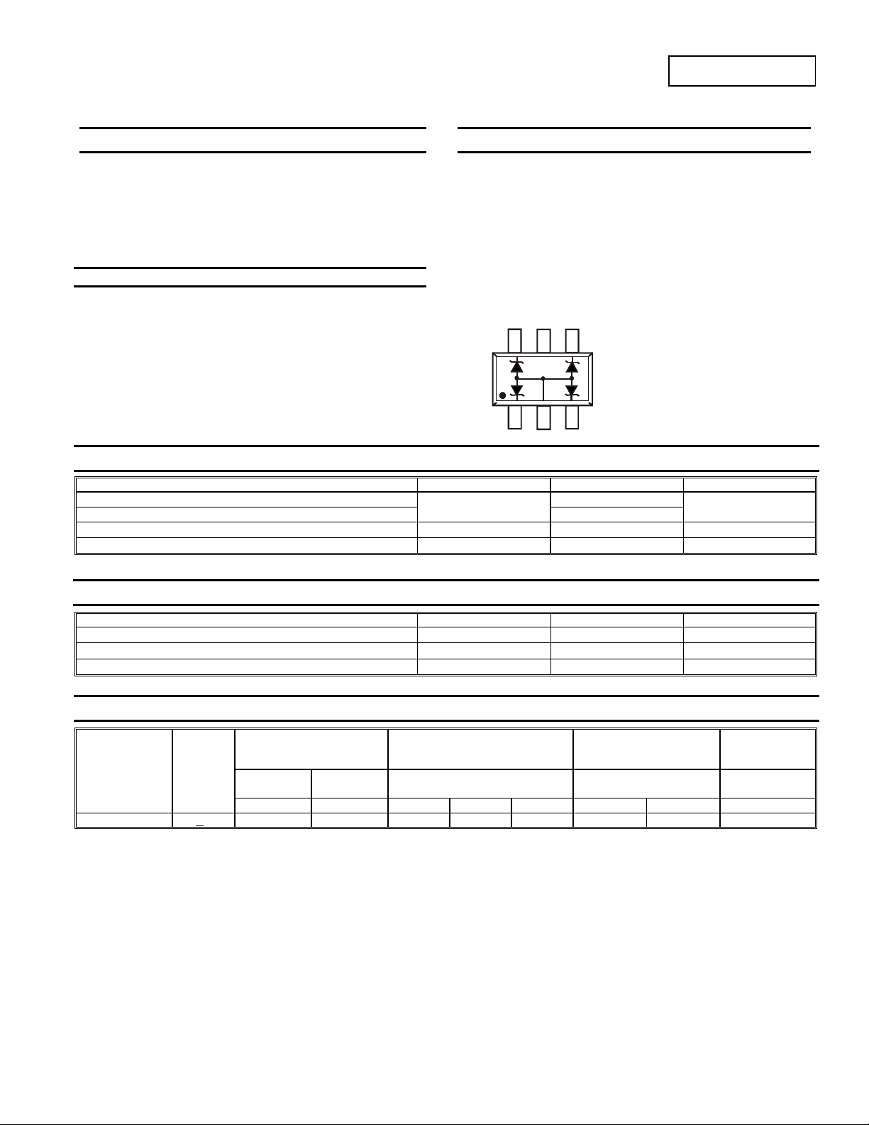
Top View
= 25°C unless otherwise specified
A
Bottom View
Characteristic Symbol Value Unit
Peak Power Dissipation, 10x1000μS Waveform (Note 5)
Peak Power Dissipation, 8x20μS Waveform (Note 5)
Ppk
Forward Voltage @ IF = 10mA (Note 3) VF
Forward Voltage @ IF = 100mA (Note 3) VF
QZX563C6V8C
QUAD SURFACE MOUNT TVS ARRAY
Rating 94V-0
Solderable per MIL-STD-202, Method 208
NC
C
1
C
4
Device Schematic
C
2
AC
3
10
80
0.9 V
1.0 V
W
Thermal Characteristics
Characteristic Symbol Value Unit
Power Dissipation (Note 4)
Thermal Resistance, Junction-to-Ambient (Note 4)
Operating and Storage Temperature Range
Electrical Characteristics @T
Reverse Standoff Voltage
Type
Number
QZX563C6V8C CB 5 1.5 6.47 6.8 7.14 1.0 3.0 63
Notes: 1. No purposefully added lead.
2. Diodes Inc.'s "Green" policy can be found on our website at http://www.diodes.com/products/lead_free/index.php.
3. Short duration pulse test used to minimize self-heating effect.
4. Device mounted on FR-4 PCB, 1 inch x 0.85 inch x 0.062 inch; pad layout as shown on Diodes Inc. Suggested Pad Layout Document AP02001,
which can be found on our website at http://www.diodes.com/datasheets/ap02001.pdf.
5. Non-repetitive current pulse per Figure 2 & 3 and derate above T
QZX563C6V8C
Document number: DS30716 Rev. 4 - 2
Marking
Code
V
RWM
= 25°C unless otherwise specified
A
and Leakage
IR @ V
V
RWM
μA
PD
R
JA
θ
T
J, TSTG
Breakdown Voltage
(Note 3)
V
@ IT = 1mA IR @ VR
BR
Min (V) Nom (V) Max (V)
= 25°C per Figure 1.
A
1 of 3
www.diodes.com
150 mW
833 °C/W
-65 to +150
Maximum Reverse
Current
(Note 3)
μA
V
°C
Typical Junction
Capacitance
CT @ VR = 0V,
f = 1MHz
pF
July 2008
© Diodes Incorporated
Page 2
P
P
U
RATIN
G
N
O
TEST
C
URR
N
T
C, T
O
T
CAPACIT
C
QZX563C6V8C
100
F
%
75
100
I
50
LSE DE
25
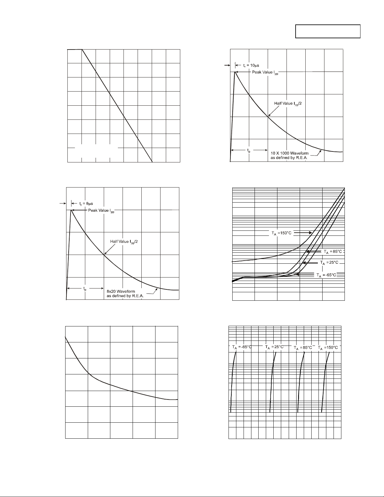
PEAK POWER OR CURRENT
EAK
10 X 1000 Waveform
as defined by R.E.A.
0
0 25 50 75 100 125 150 175 200
T , AMBIENT TEMPERATURE (°C)
A
Fig. 1 Pulse Derating Curve
50
PP pp
I , PEAK PULSE CURRENT (%I )
0
012
t, TIME (ms)
Fig. 2 Pulse Waveform
3
1
I , PEAK PULSE CURRENT (%I )
E (pF)
AN
AL
100
PP pp
T
50
70
60
50
40
30
20
10
0.1
0.01
0.001
R
I , LEAKAGE CURRENT (µA)
0
0
20 40
60
t, TIME (ms)
Fig. 3 Pulse Waveform
0.0001
1
2
V , REVERSE VOLTAGE (V)
345
R
Fig. 4 Typical Leakag e C ur r ent vs. Reve r se Vol t age
6
100
(mA)
10
E
1
T
I,
0
012
V , REVERSE VOLT AGE (V)
R
3
Fig. 5 Typical Total Capacitance vs. Reverse Voltage
4
5
0.1
6.5 6.75 7 7.25
V , BREAKDOWN VOLTAGE (V)
BR
Fig. 6 Brea kdown Voltage vs. Test Current
QZX563C6V8C
Document number: DS30716 Rev. 4 - 2
2 of 3
www.diodes.com
July 2008
© Diodes Incorporated
Page 3

QZX563C6V8C
Ordering Information (Note 6)
Part Number Case Packaging
QZX563C6V8C-7 SOT-563 3000/Tape & Reel
Notes: 6. For packaging details, go to our website at http://www.diodes.com/datasheets/ap02007.pdf.
Marking Information
Date Code Key
Year 2005 2006 2007 2008 2009 2010 2011 2012 2013 2014 2015
Code S T U V W X Y Z A B C
Month Jan Feb Mar Apr May Jun Jul Aug Sep Oct Nov Dec
Code 1 2 3 4 5 6 7 8 9 O N D
CB
YM
CB = Product Type Marking Code
YM = Date Code Marking
Y = Year (Ex: S = 2005)
M = Month (ex: 9 = September)
Package Outline Dimensions
K
A
SOT-563
Dim
Min Max Typ
B
C
D
G
M
H
L
A 0.15 0.30 0.20
B 1.10 1.25 1.20
C 1.55 1.70 1.60
D - - 0.50
G 0.90 1.10 1.00
H 1.50 1.70 1.60
K 0.55 0.60 0.60
L 0.10 0.30 0.20
M 0.10 0.18 0.11
All Dimensions in mm
Suggested Pad Layout
Diodes Incorporated and its subsidiaries reserve the right to make modifications, enhancements, improvements, corrections or other changes
without further notice to any product herein. Diodes Incorporated does not assume any liability arising out of the application or use of any product
described herein; neither does it convey any license under its patent rights, nor the rights of others. The user of products in such applications shall
assume all risks of such use and will agree to hold Diodes Incorporated and all the companies whose products are represented on our website,
harmless against all damages.
Diodes Incorporated products are not authorized for use as critical components in life support devices or systems without the expressed written
approval of the President of Diodes Incorporated.
G
Z
Y
X
QZX563C6V8C
Document number: DS30716 Rev. 4 - 2
EE
Dimensions Value (in mm)
Z 2.2
G 1.2
C
IMPORTANT NOTICE
LIFE SUPPORT
3 of 3
www.diodes.com
X 0.375
Y 0.5
C 1.7
E 0.5
July 2008
© Diodes Incorporated
 Loading...