

Page 1
A
Please click here to visit our online spice models database.
QUAD SURFACE MOUNT ZENER DIODE ARRAY
Features
• Nominal Zener Voltages: 5.6V, 6.8V, 12V, 15V, 20V
• Ultra-Small Surface Mount Package
• Ideal For Transient Suppression
• Lead Free/RoHS Compliant (Note 4)
• "Green" Device (Note 5 and 6)
Maximum Ratings @T
= 25°C unless otherwise specified
A
Single phase, half wave, 60Hz, resistive or inductive load.
For capacitance load, derate current by 20%.
Characteristic Symbol Value Unit
Forward Voltage (Note 1) @ IF = 10mA VF
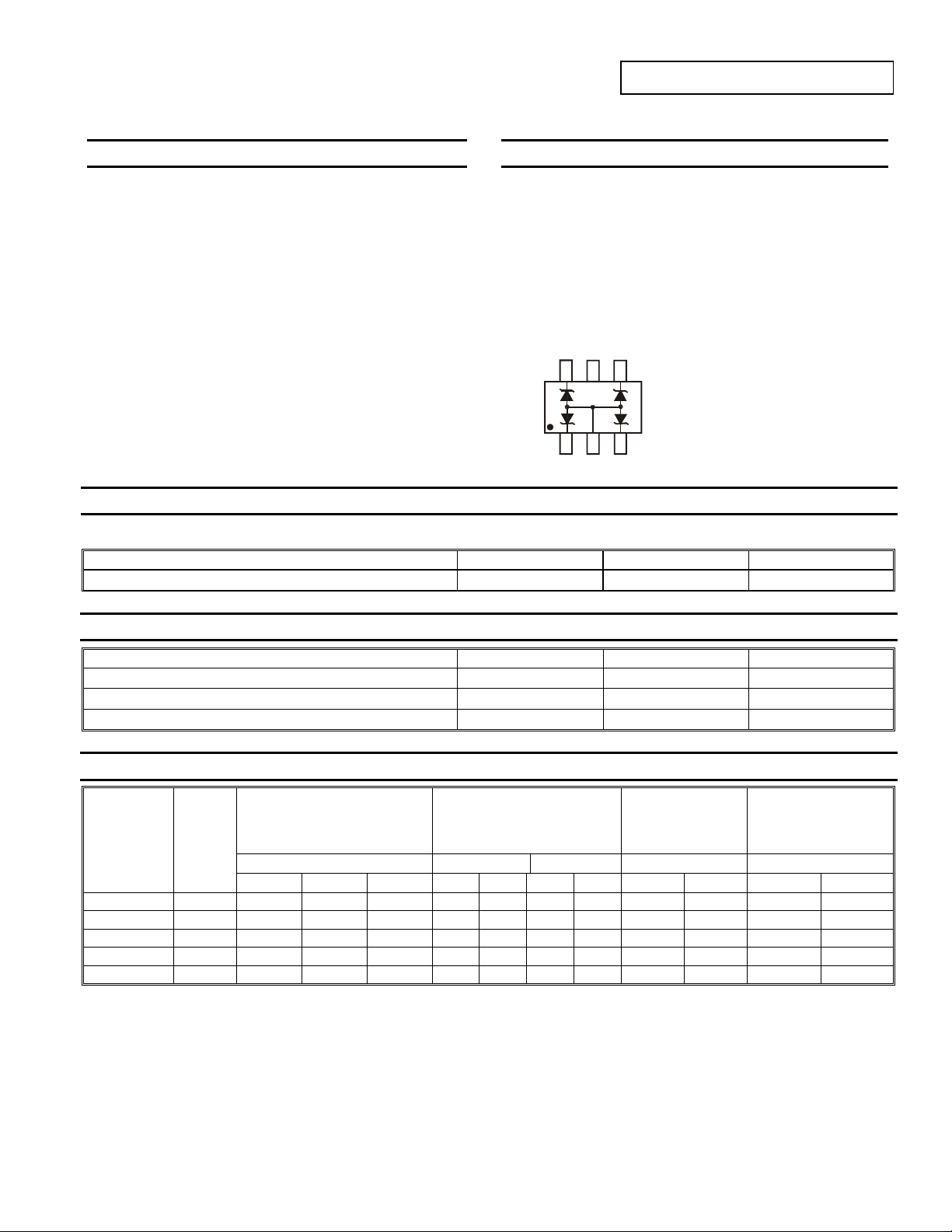
Top View Device Schematic
Mechanical Data
• Case: SOT-363
• Case Material: Molded Plastic. UL Flammability Classification
• Moisture Sensitivity: Level 1 per J-STD-020D
• Terminals: Solderable per MIL-STD-202, Method 208
• Lead Free Plating (Matte Tin Finish annealed over Alloy 42
• Orientation: See Diagram
• Marking Information: See Page 3
• Ordering Information: See Page 3
• Weight: 0.006 grams (approximate)
Rating 94V-0
leadframe).
NC
C
1
C
4
QZX363C5V6 - QZX363C20
C
2
C
3
0.9 V
Thermal Characteristics
Characteristic Symbol Value Unit
Power Dissipation
Thermal Resistance, Junction to Ambient Air (Note 3)
Operating and Storage Temperature Range (Note 3)
Electrical Characteristics @T
Type
Number
QZX363C5V6 K5F 5.6 5.32 5.88 40 5.0 400 1.0 1.0 2.0 -2.0 2.5
QZX363C6V8 K6F 6.8 6.47 7.14 15 5.0 80 1.0 2.0 4.0 1.2 4.5
QZX363C12 KFF 12 11.4 12.7 25 5.0 150 1.0 0.1 8.0 6.0 10.0
QZX363C15 KJF 15 13.8 15.6 30 5.0 200 1.0 0.1 10.5 9.2 13.0
QZX363C20 KMF 20 19.0 21.0 55 5.0 225 1.0 0.1 14 14.4 18.0
Notes: 1. Short duration pulse test used to minimize self-heating effect.
http://www.diodes.com/datasheets/ap02001.pdf.
DQZX363C5V6-QZX363C20
Document number: DS30143 Rev. 13 - 2
Marking
Code
V
Nom (V) Min (V) Max (V)
2. f = 1KHz.
3. Device mounted on FR-4 PC board with recommended pad layout, which can be found on our website at
4. No purposefully added lead.
5. Diodes Inc.'s "Green" policy can be found on our website at http://www.diodes.com/products/lead_free/index.php.
6. Product manufactured with Date Code UO (week 40, 2007) and newer are built with Green Molding Compound. Product manufactured prior to Date
Code UO are built with Non-Green Molding Compound and may contain Halogens or Sb2O3 Fire Retardants.
A
Zener Voltage
Range (Note 1)
Z @ IZT =
PD
R
JA
θ
T
J, TSTG
= 25°C unless otherwise specified
Maximum Zener Impedance
(Note 2)
5.0mA ZZT @ IZT Z
mA
Ω
1 of 4
www.diodes.com
ZK @ IZK
Ω
200 mW
625 °C/W
-65 to +150
Temperature
Maximum Reverse
Current (Note 1)
Coefficient of
Zener Voltage
@ IZT = 5mA
IR @ VR TC (mV/°C)
mA
μA
V Min Max
© Diodes Incorporated
°C
June 2008
Page 2
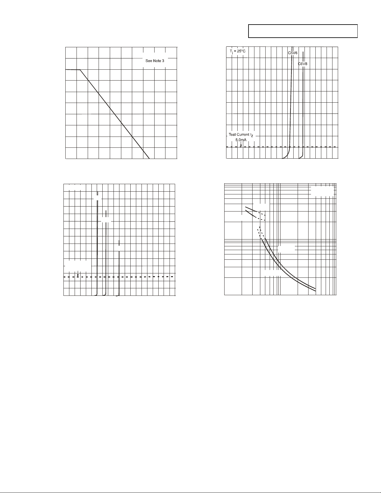
P, P
OWER
PATIO
N
R CUR
RENT
R CUR
RENT
QZX363C5V6 - QZX363C20
250
200
(mW)
150
DISSI
100
D
50
30
(mA)
20
0
0
T , AMBIENT TEMPERATURE (°C)
A
Fig. 1 Power Derating Curve
T = 25°C
j
C12
C15
100
200
50
40
(mA)
30
20
Z
I, ZENE
10
0
01 2345 67891
V , ZENER VOLTAGE (V)
Z
Fig. 2 Typical Zener Breakdown Characteristics
1,000
V = 1V
R
V = 2V
R
T= 25 °C
j
0
100
C20
10
Test current I
Z
I, ZENE
0
0
Fig. 3 Typical Zener Breakdown Characteristics
Z
5mA
10 20 30 40
V , ZENER VOLTAGE (V)
Z
T
C , TOTAL CAPACITANCE (pF)
10
1
V , NOMINAL ZENER VOLTAGE (V)
Fig. 4 Typical Total Capacitance vs. Nominal Zener Voltage
Z
V = 1V
R
V = 2V
R
10 100
DQZX363C5V6-QZX363C20
Document number: DS30143 Rev. 13 - 2
2 of 4
www.diodes.com
June 2008
© Diodes Incorporated
Page 3

QZX363C5V6 - QZX363C20
Ordering Information (Note 7)
Device Packaging Shipping
QZX363C5V6-7-F SOT-363 3000/Tape & Reel
QZX363C6V8-7-F SOT-363 3000/Tape & Reel
QZX363C12-7-F SOT-363 3000/Tape & Reel
QZX363C15-7-F SOT-363 3000/Tape & Reel
QZX363C20-7-F SOT-363 3000/Tape & Reel
Notes: 7. For packaging details, go to our website at http://www.diodes.com/datasheets/ap02007.pdf.
Marking Information
Date Code Key
Year 2000 2001 2002 2003 2004 2005 2006 2007 2008 2009 2010 2111 2012
Code L M N P R S T U V W X Y Z
Month Jan Feb Mar Apr May Jun Jul Aug Sep Oct Nov Dec
Code 1 2 3 4 5 6 7 8 9 O N D
xxx
xxx= Product Type Marking Code
(See Electrical Characteristics Table)
YM = Date Code Marking
YM
Y = Year (ex: N = 2002)
M = Month (ex: 9 = September)
Package Outline Dimensions
A
K
J
H
D
Suggested Pad Layout
G
Z
Y
X
SOT-363
Dim Min Max
B C
M
L
F
EE
C
A 0.10 0.30
B 1.15 1.35
C 2.00 2.20
D 0.65 Nominal
F 0.40 0.45
H 1.80 2.20
J 0 0.10
K 0.90 1.00
L 0.25 0.40
M 0.10 0.22
α
All Dimensions in mm
Dimensions Value (in mm)
Z 2.5
G 1.3
X 0.42
Y 0.6
C 1.9
E 0.65
0° 8°
DQZX363C5V6-QZX363C20
Document number: DS30143 Rev. 13 - 2
3 of 4
www.diodes.com
June 2008
© Diodes Incorporated
Page 4

IMPORTANT NOTICE
Diodes Incorporated and its subsidiaries reserve the right to make modifications, enhancements, improvements, corrections or other changes
without further notice to any product herein. Diodes Incorporated does not assume any liability arising out of the application or use of any product
described herein; neither does it convey any license under its patent rights, nor the rights of others. The user of products in such applications shall
assume all risks of such use and will agree to hold Diodes Incorporated and all the companies whose products are represented on our website,
harmless against all damages.
LIFE SUPPORT
Diodes Incorporated products are not authorized for use as critical components in life support devices or systems without the expressed written
approval of the President of Diodes Incorporated.
QZX363C5V6 - QZX363C20
DQZX363C5V6-QZX363C20
Document number: DS30143 Rev. 13 - 2
4 of 4
www.diodes.com
June 2008
© Diodes Incorporated
 Loading...