DIODES P4KE10CA, P4KE110C, P4KE120A, P4KE12A, P4KE120C Datasheet
...
DS21508 Rev. B-4 1 of 4 P4KE6.8-P4KE400CA
P4KE6.8 - P4KE400CA
TRANSIENT VOLTAGE SUPPRESSOR
·
UL Recognized
·
400W Peak Pulse Power Dissipation
·
Voltage Range 6.8V - 400V
·
Constructed with Glass Passivated Die
·
Uni and Bidirectional Versions Available
·
Excellent Clamping Capability
·
Fast Response Time
Maximum Ratings
@ TA= 25°C unless otherwise specified
Characteristic Symbol Value Unit
Peak Power Dissipation, Tp= 1.0 ms (Non repetitive current pulse,
per Figure 1 and derated above T
A
= 25°C per Figure 4)
P
pk
400 W
Steady State Power Dissipation at TL= 75°C
Lead Lengths 9.5 mm per Figure 5 (Mounted on Copper Land Area of 40mm
2
)
P
d
1.0 W
Peak Forward Surge Current, 8.3 ms Single Half Sine Wave, Superimposed
on Rated Load (JEDEC Method) Duty Cycle = 4 pulses per minute maximum)
I
FSM
40 A
Forward Voltage @ IF= 20A VBR£ 200V
300µs Square Wave Pulse, Unidirectional Only V
BR
> 200V
V
F
3.5
6.5
V
Operating and Storage Temperature Range
T
j
, T
STG
-55 to +175 °C
Features
·
Case: Transfer Molded Epoxy
·
Leads: Plated Leads, Solderable per
MIL-STD-202, Method 208
· Marking: Unidirectional - Type Number and
Cathode Band
· Marking: Bidirectional - Type Number Only
· Approx. Weight: 0.4 grams
· Mounting Position: Any
Mechanical Data
A
A
B
C
D
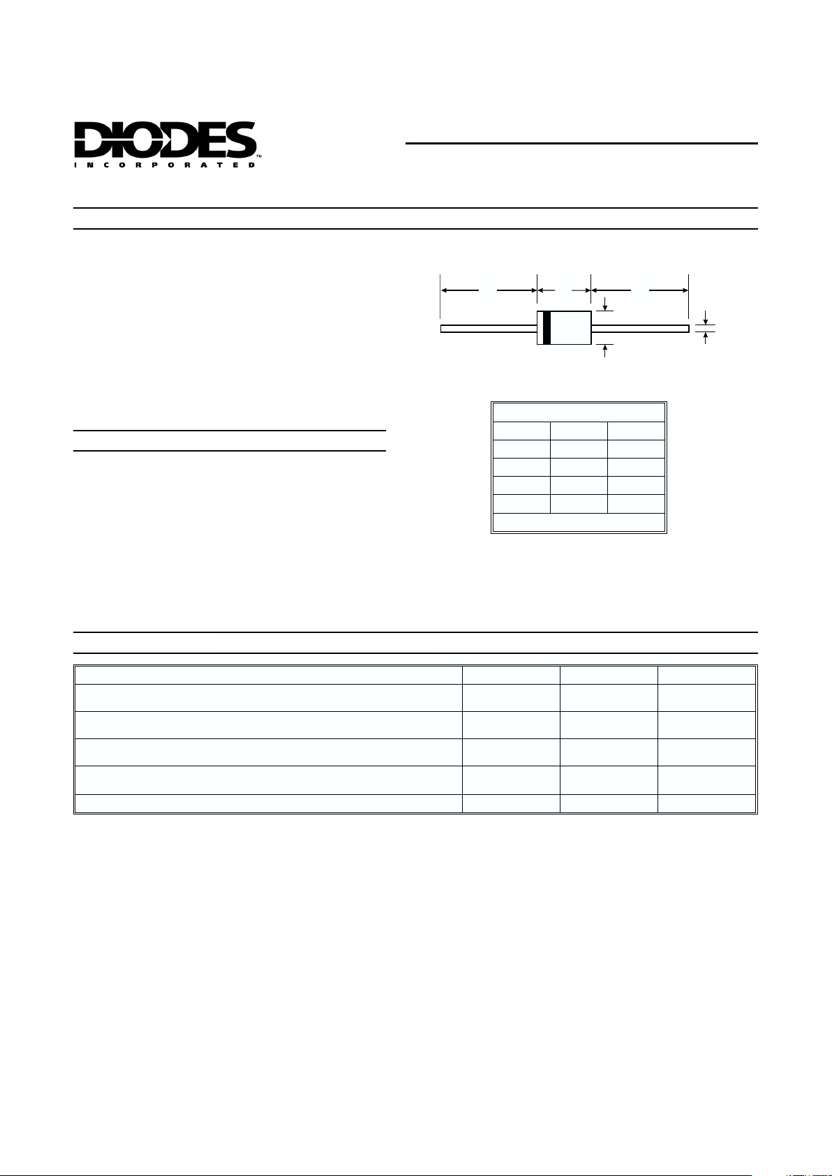
DO-41
Dim Min Max
A
25.40 —
B
4.06 5.21
C
0.71 0.884
D
2.00 2.72
All Dimensions in mm

DS21508 Rev. B-4 2 of 4 P4KE6.8-P4KE400CA
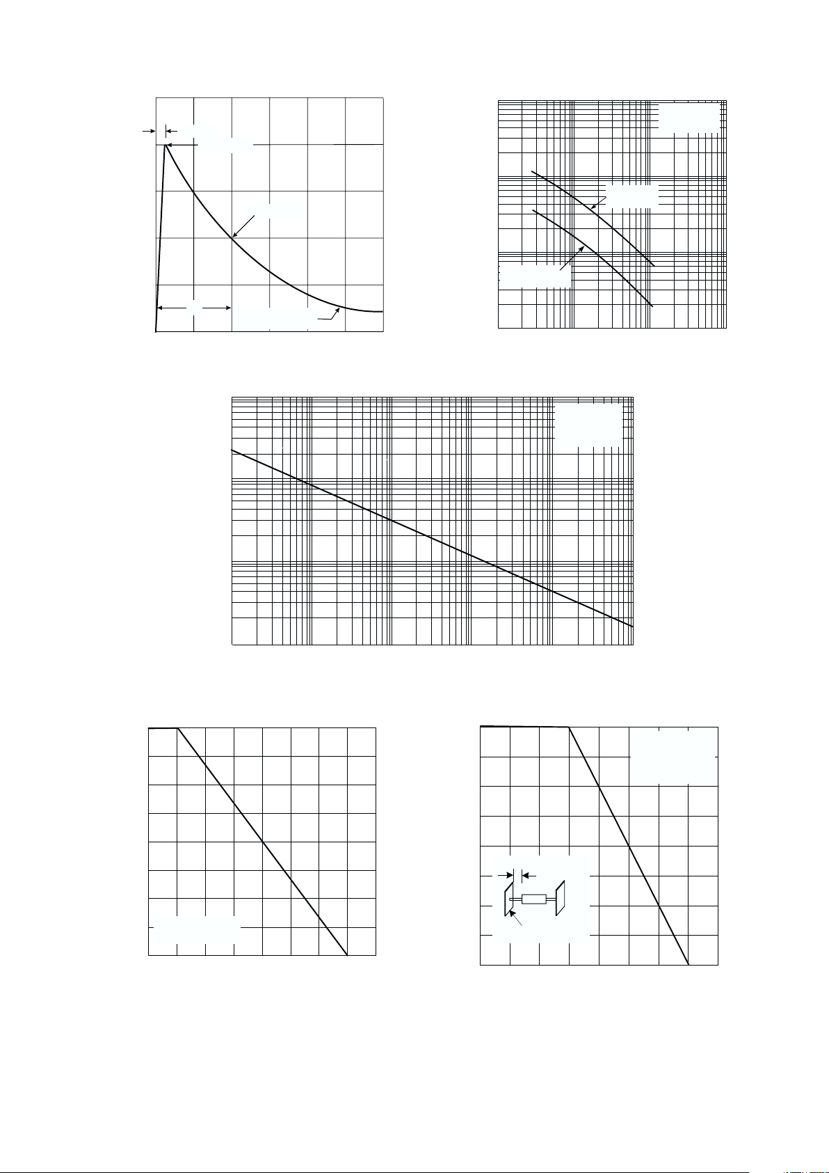
10 X 1000 Waveform
as defined by REA
0 25 50 75 100 125 150 175 200
100
75
50
25
0
T , AMBIENT TEMPERATURE (°C)
Fi
g
. 4 Pulse DeratingCurve
A
PK PULSE DERATING (% PK PWR OR CURRENT
)
L = 9.5 mm
40x40x1mmCu
0
25 50 75 100 125 150 175
200
0
T , LEAD TEMPERATURE (°C)
Fi
g
. 5, SteadyState Power Deratin
g
L
P , STEADY STATE POWER DISSIPATION (W)
d
Single Phase
Half-Wave 60Hz
Resistive or
Inductive Load
0.25
0.5
0.75
1.0
0.1 1.0
T , PULSE WIDTH (µs)
Fi
g
. 3 Pulse RatingCurve
p
0.1
10 100
1.0
10
100
1000 10000
P , PEAK PULSE POWER (kW)
P
Non-Repetitive
Pulse Waveform
Shown in Fig. 1
T = 25°C
A
012
3
100
50
0
I , PEAK PULSE CURRENT (% )
Ppp
t = 10ms
r
Peak Value I
pp
Half Value I /2
pp
10 X 1000 Waveform
as defined by R.E.A.
t
p
t, TIME (ms)
Fi
g
. 1 Pulse Waveform
1 10 100 1000
100
1000
10,000
100,000
V , REVERSE STANDOFF VOLTAGE (V)
Fi
g
.2Typical Junction Capacitance
RWM
C , CAPACITANCE (pF)
j
Measured at
Stand-off Voltage
Measured at
Zero Bias
T = 25°C
j
f = 1.0 MHz
V = 50mV p-p
sig
Notes: 1. Suffix ‘C’ denotes bidirectional device. Suffix ‘A’ denotes 5% tolerance device, no suffix denotes 10% tolerance device.
2. For bidirectional devices having V
R
of 10 volts and under, the IRlimit is doubled.
3. Type Number marking may contain a “V” or dash in place of decimal point.
 Loading...