Diodes NIS5132 User Manual

Green
3.6A 12V RESETTABLE ELECTRONIC FUSE
Description
The NIS5132 is a self-protected resettable electronic fuse designed
for consumer applications such as hard disk drive to industrial
application to enhance system reliability against catastrophic and
shutdown failures.
To support a wide range of demanding applications, the design has
been optimized to operate over the supply range of 9.0V to 18V. For
robustness and protections, the device integrates a low Rdson
NMOS buffer power device along with an under voltage lockout,
overvoltage clamp, a current limit, a dv/dt control and a thermal
shutdown circuits. The overvoltage circuit limits the output voltage
without shutting the device down to allow the load to continue
operating during over voltage. Thermal shutdown can be either
latching type (NIS5132MN1) or auto-retry type (NIS5132MN2).
NEW PRODUCT
Features
• 9.0 to 18V operating input voltage
• Integrated NMOS power device with R
• Internal current limit - no external current sense resistor in load
path
• Under voltage lockout
• Over voltage clamp (NIS5132MN1 and NIS5132MN2)
• Thermal shutdown
• -40°C to +150°C operating junction temperature
• ESD ratings : HBM > 1500V; MM 200V
• Small low profile U-DFN3030-10 packages
• Lead-Free Finish; RoHS Compliant (Notes 1 & 2)
• Halogen and Antimony Free. “Green” Device (Note 3)
Notes: 1. EU Directive 2002/95/EC (RoHS) & 2011/65/EU (RoHS 2) compliant. All applicable RoHS exemptions applied.
2. See http://www.diodes.com/quality/lead_free.html for more information about Diodes Incorporated’s definitions of Halogen- and Antimony-free,
"Green” and Lead-free.
3. Halogen- and Antimony-free "Green” products are defined as those which contain <900ppm bromine, <900ppm chlorine (<1500ppm total Br + Cl)
and <1000ppm antimony compounds.
of 30mΩ typical
DS(ON)
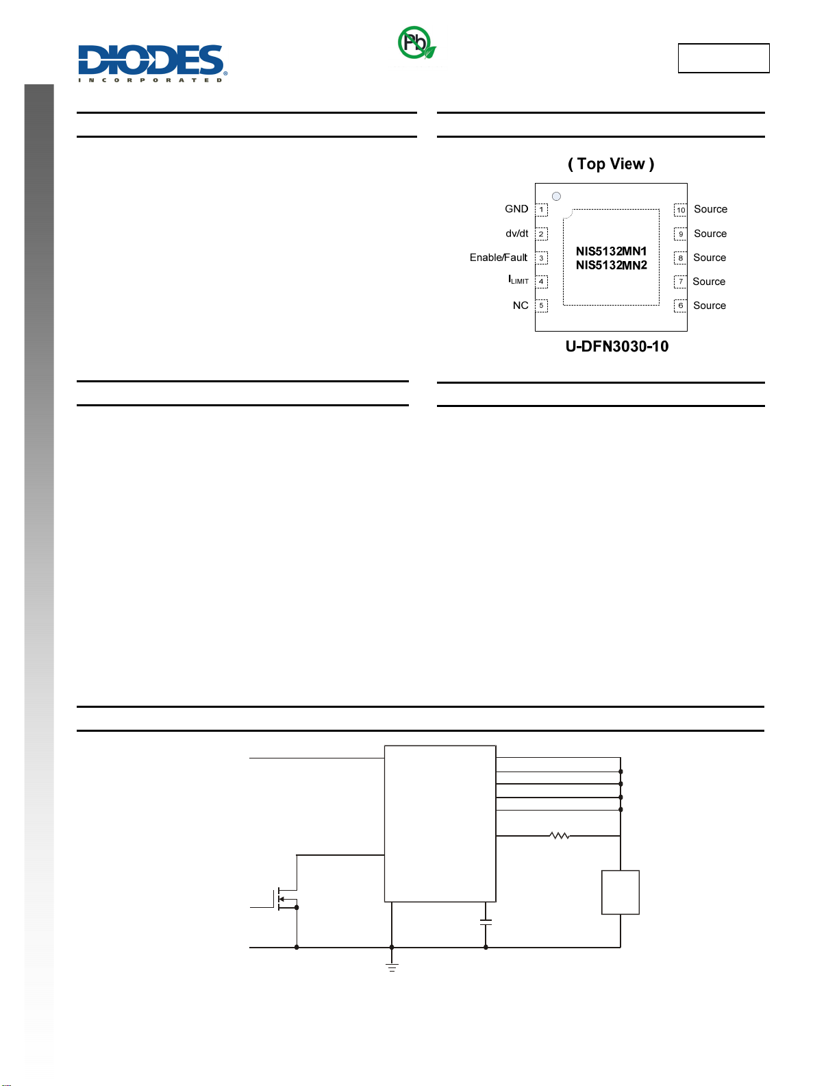
Pin Assignments
Applications
• Hard drives
• Mother board power management
• Printer load power management
Typical Application Circuits
NIS5132
+12V
ENABLE
GND
NIS5132
Document number: DS36457 Rev. 1 - 2
11
V
DD
SOURCE
NIS5132
3
ENABLE
GND dv/dt
12
I
LIMIT
10
9
8
7
6
R
4
S
LOAD
Figure 1 Application Circuit with Direct Current Sensing
1 of 11
www.diodes.com
December 2013
© Diodes Incorporated

Typical Application Circuits (cont.)
NIS5132
NEW PRODUCT
+12V
ENABLE
GND
11
V
DD
SOURCE
NIS5132
3
ENABLE
GND dv/dt
12
I
LIMIT
10
9
8
7
6
R
S
4
LOAD
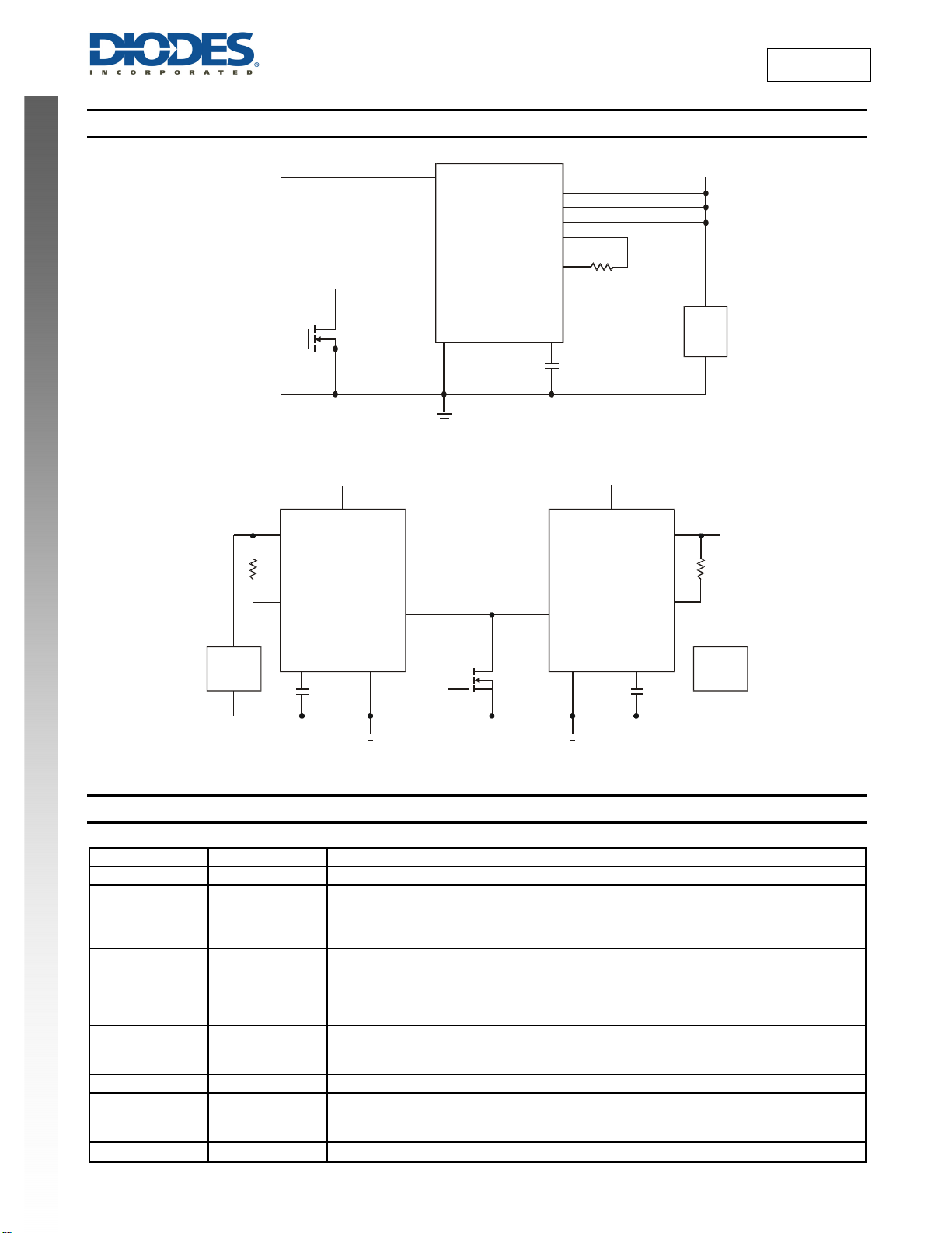
Figure 2 Application Circuit with Kelvin Current Sensing
SOURCE
I
LIMIT
V
DD
NIS5132
ENABLE
ENABLE
V
DD
NIS5132
SOURCE
I
LIMIT
R
S
LOAD
GNDdv/dt
ENABLE
Figure 3 Application Circuit with Common Thermal Shutdown
GND dv/dt
Pin Descriptions
Package: U-DFN3030-10
Pin Number Pin Name Function
1 GND Ground pin
Internal NMOS power device turn-on time adjustment pin:
2 dv/dt
3 Enable/Fault
4
5 NC No connect
6 to 10 Source
Exposed PAD
I
LIMIT
V
DD
If this pin is is left unconnected, the internal capacitor ensures the turn-on ramp is over a
period of 2ms typical. If an additional delay is required, connect a capacitor from this pin to the
ground.
Tri-state bi-directional interface pin:
The output can be disabled by pulling this pin to ground through an open drain or an open
collector. Additionally, this pin output goes to an intermediate state to indicate that the device
is in thermal shutdown state. This pin can also be connected together with other NIS5132
devices to cause a system-wide simultaneous shutdown during thermal events.
Current limit setting pin:
A resistor between Source pins and this pin sets the overload and short-circuit current limit
thresholds.
The internal NMOS power device’s Source pins:
These pins are the Source of internal power device and also the output terminal of the
electronic fuse
Positive input voltage to the device
LOAD
NIS5132
Document number: DS36457 Rev. 1 - 5
2 of 11
www.diodes.com
December 2013
© Diodes Incorporated

Functional Block Diagram
NIS5132
V
DD
NEW PRODUCT
ENABLE/
FAULT
EN/Fault
Enable
Thermal
Shutdown
UVLO
4.3V
12µA
Charge
Pump
Current
Limit
Voltage
Clamp
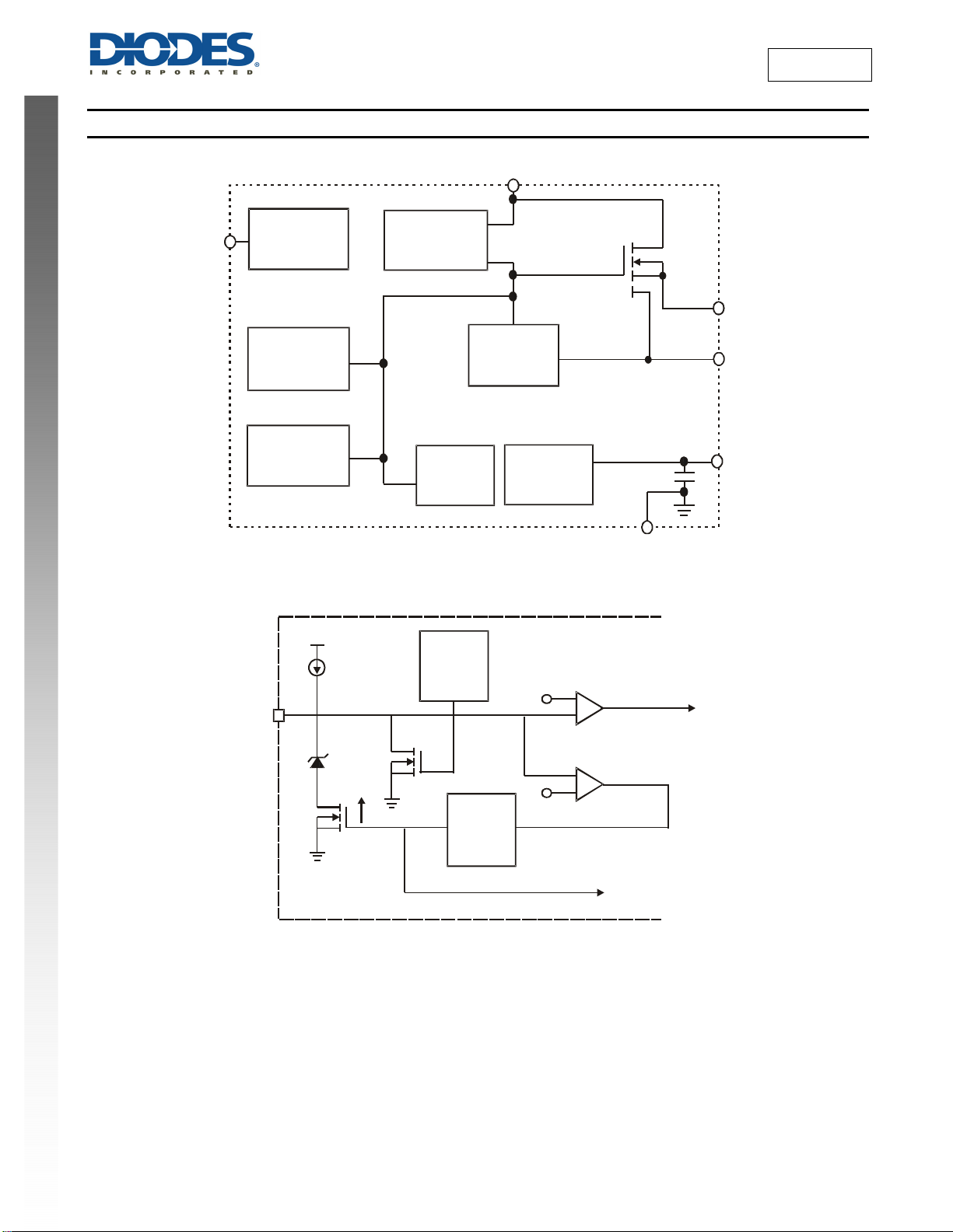
Figure 4 Block Diagram
dv/dt
Control
Startup
Blanking
2.64V
SOURCE
I
LIMIT
dv/dt
GND
+
Enable SD
-
NIS5132
Document number: DS36457 Rev. 1 - 5
1.4V
0.58V
SD
Figure 5 Enable/Fault Function Circuit
Thermal
Shutdown
3 of 11
www.diodes.com
-
+
Thermal Reset
Thermal SD
December 2013
© Diodes Incorporated

Absolute Maximum Ratings (Note 4) (@T
Symbol Characteristic Value Unit
VDD
θJA
θJL
θJC
P
DMAX
Ts Storage temperature range -55 to +155
TJ
TL
Notes: 4. Stresses greater than the 'Absolute Maximum Ratings' specified above may cause permanent damage to the device. These are stress ratings
only; functional operation of the device at these or any other conditions exceeding those indicated in this specification is not implied. Device
reliability may be affected by exposure to absolute maximum rating conditions for extended periods of time.
NEW PRODUCT
5. Negative voltage will not damage the device provided that the power dissipation is within the package package dissipation rating.
6. 1 oz copper on double sided FR4 PCB
7. Thermal limit is set above the maximum thermal rating. It is not recommended to operate the device at temperature above the maximum rating
for extended period.
Input voltage in steady state operating conditions (Note 5) -0.6 to +18
Input voltage - transient (100ms) -0.6 to +25
Junction to air thermal resistance
Junction to lead thermal resistance 27
Junction to case thermal resistance 20
Package Power Dissipation at TA= +25°C
Thermal derating above +25°C
Operating junction temperature (Note 7) -40 to +150
Lead temperature during soldering (10s) 260
= +25°C, unless otherwise specified.)
A
2
0.1 in
(Note 6) 227
0.5 in2 (Note 6) 95
1.3 W
10.4 (TBD)
Recommended Operating Conditions
NIS5132
V
°C/W
mW/°C
°C
°C
°C
Symbol Characteristic Test Condition Rating Unit
VDD
TJ
Supply Voltage Operating 9.0 to 18.0 V
Operating Juntion Temperature Range Operating -40 to +150
°C
NIS5132
Document number: DS36457 Rev. 1 - 5
4 of 11
www.diodes.com
December 2013
© Diodes Incorporated
 Loading...