Diodes MMST5401 User Manual

C
Features
• Epitaxial Planar Die Construction
• Ultra-Small Surface Mount Package
• Complementary PNP Type: MMST5551
• Ideal for Low Power Amplification and Switching
• Totally Lead-Free & Fully RoHS compliant (Notes 1 & 2)
• Halogen and Antimony Free. “Green” Device (Note 3)
• Qualified to AEC-Q101 Standards for High Reliability
• PPAP Capable (Note 4)
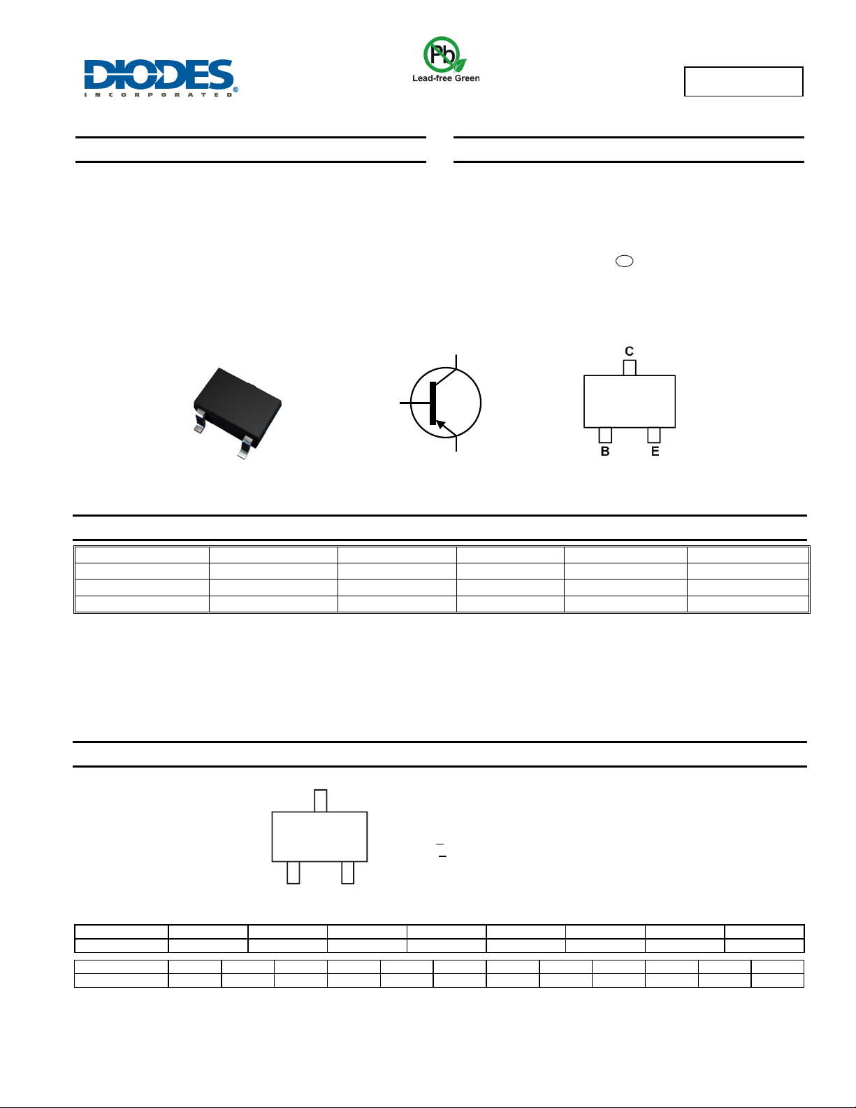
SOT323
Top View
Ordering Information (Notes 4 & 5)
B
Device Symbol
MMST5401
160V PNP SMALL SIGNAL TRANSISTOR IN SOT323
Mechanical Data
• Case: SOT323
• Case Material: Molded Plastic. “Green” Molding Compound.
UL Flammability Rating 94V-0
• Moisture Sensitivity: Level 1 per J-STD-020
• Terminals: Finish - Matte Tin Plated Leads, Solderable per
MIL-STD-202, Method 208
• Weight: 0.006 grams (approximate)
E
e3
Top View
Pin-Out
Device
MMST5401-7-F
MMST5401-13-F
MMST5401Q-7-F
Notes: 1. No purposely added lead. Fully EU Directive 2002/95/EC (RoHS) & 2011/65/EU (RoHS 2) compliant.
2. See http://www.diodes.com/quality/lead_free.html for more information about Diodes Incorporated’s definitions of Halogen- and Antimony-free, "Green"
and Lead-free.
3. Halogen- and Antimony-free "Green” products are defined as those which contain <900ppm bromine, <900ppm chlorine (<1500ppm total Br + Cl) and
<1000ppm antimony compounds.
4. Automotive products are AEC-Q101 qualified and are PPAP capable. Automotive, AEC-Q101 and standard products are electrically and thermally
the same, except where specified. For more information, please refer to http://www.diodes.com/quality/product_compliance_definitions/.
5. For packaging details, go to our website at http://www.diodes.com/products/packages.html.
Compliance Marking Reel Size (inches) Tape Width (mm) Quantity per reel
AEC-Q101 K4M 7 8 3,000
AEC-Q101 K4M 13 8 10,000
Automotive K4M 7 8 3,000
Marking Information
Date Code Key
xxx
Year 2010 2011 2012 2013 2014 2015 2016 2017
Code X Y Z A B C D E
Month Jan Feb Mar Apr May Jun Jul Aug Sep Oct Nov Dec
Code 1 2 3 4 5 6 7 8 9 O N D
YM
K4M = Product Type Marking Code
YM = Date Code Marking
Y or Y = Year (ex: A = 2013)
M or M = Month (ex: 9 = September)
MMST5401
Document number: DS30170 Rev. 10 - 2
1 of 4
www.diodes.com
May 2014
© Diodes Incorporated

V
V
V
Absolute Maximum Ratings (@T
= +25°C, unless otherwise specified.)
A
Characteristic Symbol
Collector-Base Voltage
Collector-Emitter Voltage
Emitter-Base Voltage
Continuous Collector Current
Thermal Characteristics (@T
= +25°C, unless otherwise specified.)
A
Characteristic Symbol
Power Dissipation (Note 6)
Thermal Resistance, Junction to Ambient (Note 6)
Operating and Storage Temperature Range
ESD Ratings (Note 7)
R
T
J,TSTG
MMST5401
alue Unit
V
CBO
V
CEO
V
EBO
IC
P
D
θJA
-160 V
-150 V
-5.0 V
-200 mA
alue Unit
200 mW
625
-55 to +150
°C/W
°C
Characteristic Symbol
alue Unit JEDEC Class
Electrostatic Discharge - Human Body Model ESD HBM 4,000 V 3A
Electrostatic Discharge - Machine Model ESD MM 400 V C
Electrical Characteristics (@T
= +25°C, unless otherwise specified.)
A
Characteristic Symbol Min Max Unit Test Condition
OFF CHARACTERISTICS (Note 8)
Collector-Base Breakdown Voltage
Collector-Emitter Breakdown Voltage
Emitter-Base Breakdown Voltage
Collector Cutoff Current
Emitter Cutoff Current
V
V
V
I
CBO
I
EBO
CBO
CEO
EBO
-160
-150
-5.0
⎯
⎯
⎯
⎯
⎯
-50
-50 nA
V
IC = -100μA, IE = 0
V
IC = -1.0mA, IB = 0
V
IE = -10μA, IC = 0
VCB = -120V, IE = 0
nA
µA
VCB = -120V, IE = 0, TA = +100°C
VEB = -3.0V, IC = 0
ON CHARACTERISTICS (Note 8)
DC Current Gain
Collector-Emitter Saturation Voltage
Base-Emitter Saturation Voltage
hFE
V
CE(SAT)
V
BE(SAT)
50
60
50
⎯
⎯
⎯
240
⎯
-0.2
-0.5
-1.0 V
IC = -1.0mA , VCE = -5.0V
IC = -10mA, VCE = -5.0V
⎯
IC = -50mA, VCE = -5.0V
IC = -10mA, IB = -1.0mA
V
IC = -50mA, IB = -5.0mA
IC = -10mA, IB = -1.0mA
IC = -50mA, IB = -5.0mA
SMALL SIGNAL CHARACTERISTICS
Output Capacitance
Small Signal Current Gain
Current Gain-Bandwidth Product
C
obo
hfe
fT
Noise Figure NF
Notes: 6. For a device mounted on minimum recommended pad layout 1oz copper that is on a single-sided FR4 PCB; device is measured under still air
8. Measured under pulsed conditions. Pulse width ≤ 300µs. Duty cycle ≤ 2%.
conditions whilst operating in a steady-state.
7. Refer to JEDEC specification JESD22-A114 and JESD22-A115.
⎯
40 200
100 300 MHz
⎯
6.0 pF
⎯
8.0 dB
VCB = -10V, f = 1.0MHz, IE = 0
VCE = -10V, IC = -1.0mA,
f = 1.0kHz
VCE = -10V, IC = -10mA,
f = 100MHz
VCE = -5.0V, IC = -200µA,
RS =10Ω, f = 1.0kHz
MMST5401
Document number: DS30170 Rev. 10 - 2
2 of 4
www.diodes.com
May 2014
© Diodes Incorporated
 Loading...