DIODES MMST4126 Datasheet

Features
Epitaxial Planar Die Construction
·
Complementary NPN Type Available
·
(MMST4124)
Ideal for Medium Power Amplification and
·
Switching
Ultra-Small Surface Mount Package
·
Mechanical Data
Case: SOT-323, Molded Plastic
·
Terminals: Solderable per MIL-STD-202,
·
NEW PRODUCT
Method 208
Terminal Connections: See Diagram
·
Marking: K2B
·
Weight: 0.006 grams (approx.)
·
MMST4126
PNP SMALL SIGNAL SURFACE MOUNT TRANSISTOR
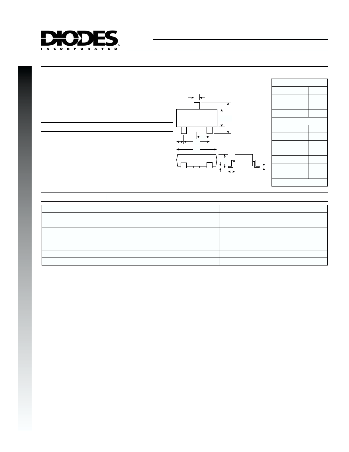
SOT-323
Dim Min Max
E
TOP VIEW
B
A
C
B
C
E
D
G
H
K
J
L
A
B
C
D
E
G
H
J
M
K
L
M
All Dimensions in mm
0.30 0.40
1.15 1.35
2.00 2.20
0.65 Nominal
0.30 0.40
1.20 1.40
1.80 2.20
0.0 0.10
0.90 1.00
0.25 0.40
0.10 0.25
Maximum Ratings
Characteristic Symbol MMST4126 Unit
Collector-Base Voltage
Collector-Emitter Voltage
Emitter-Base Voltage
Collector Current - Continuous (Note 1)
Power Dissipation (Note 1)
Thermal Resistance, Junction to Ambient (Note 1)
Operating and Storage and Temperature Range
Note: 1. Valid provided that terminals are kept at ambient temperature.
2. Pulse test: Pulse width £ 300ms, duty cycle £ 2%.
@ TA= 25°C unless otherwise specified
V
V
V
R
T
j,TSTG
CBO
CEO
EBO
I
C
P
d
qJA
-25 V
-25 V
-4.0 V
-200 mA
200
625 K/W
-55 to +150 °C
mW
DS30161 Rev. B-1 1 of 2 MMST4126

Electrical Characteristics
@ TA= 25°C unless otherwise specified
Characteristic Symbol Min Max Unit Test Condition
OFF CHARACTERISTICS (Note 2)
Collector-Base Breakdown Voltage
Collector-Emitter Breakdown Voltage
Emitter-Base Breakdown Voltage
Collector Cutoff Current
Emitter Cutoff Current
ON CHARACTERISTICS (Note 2)
DC Current Gain
NEW PRODUCT
Collector-Emitter Saturation Voltage
Base- Emitter Saturation Voltage
SMALL SIGNAL CHARACTERISTICS
Output Capacitance
Input Capacitance
Small Signal Current Gain
Current Gain-Bandwidth Product
Noise Figure
Note: 1. Valid provided that terminals are kept at ambient temperature.
2. Pulse test: Pulse width £ 300ms, duty cycle £ 2%.
V
(BR)CBO
V
(BR)CEO
V
(BR)EBO
I
CBO
I
EBO
h
V
CE(SAT)
V
BE(SAT)
C
C
h
f
FE
obo
ibo
fe
T
-25 ¾ V
-25 ¾ V
-4.0 ¾ V
¾ -50 nA
¾ -50 nA
120
60
360
¾
¾ -0.40 V
¾ -0.95 V
¾ 4.5 pF
¾ 10 pF
120 480 ¾
250 ¾ MHz
NF ¾ 4.0 dB
¾
= -10mA, IE= 0
I
C
= -1.0mA, IB= 0
I
C
= -10mA, IC= 0
I
E
V
= -20V, IE= 0V
CB
= -3.0V, IC= 0V
V
EB
= -2.0mA, VCE= -1.0V
I
C
I
= -50mA, VCE= -1.0V
C
= -50mA, IB= -5.0mA
I
C
= -50mA, IB= -5.0mA
I
C
= -5.0V, f = 1.0MHz, IE= 0
V
CB
= -0.5V, f = 1.0MHz, IC= 0
V
EB
= 1.0V, IC= -2.0mA,
V
CE
f = 1.0kHz
= -20V, IC= -10mA,
V
CE
f = 100MHz
= -5.0V, IC= -100mA,
V
CE
R
= 1.0kW, f = 1.0kHz
S
DS30161 Rev. B-1 2 of 2 MMST4126
 Loading...