

Page 1
A
1
E
1
B
A
Features & Benefits
• BV
• I
• General purpose NPN transistors ideally suited for low power
• Dual transistors in a single SOT26 package taking half the
• Epitaxial planar die construction
• “Lead Free”, RoHS Compliant (Note 1)
• Halogen and Antimony Free. "Green" Device (Note 2)
• Qualified to AEC-Q101 Standards for High Reliability
ADVANCE INFORMATION
> 80V
CEO
= 1A Peak Pulse Current
CM
amplification and switching applications
footprint of two equivalent transistors in SOT23
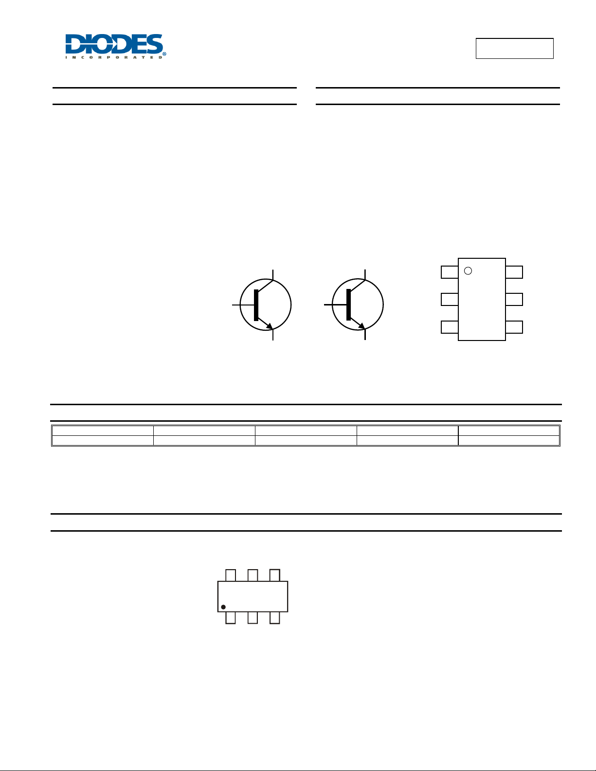
SOT26
1
Top View
MMDTA06
80V DUAL NPN SMALL SIGNAL SURFACE MOUNT TRANSISTOR
Mechanical Data
• Case: SOT26
• Case Material: Molded Plastic, “Green” Molding Compound.
UL Flammability Classification Rating 94V-0
• Moisture Sensitivity: Level 1 per J-STD-020
• Terminals: Solderable per MIL-STD-202, Method 208
• Lead Free Plating: Matte Tin Finish annealed over Copper
leadframe
• Weight: 0.015 grams (approximate)
C
B2
Device Symbol
C2
E2
B1
E2
B2
C1
E1
C2
Top View
Pin-Out
Ordering Information (Note 3)
Product Marking Reel size (inches) Tape width (mm) Quantity per reel
MMDTA06-7 A06 7 8 3,000
Notes: 1. No purposefully added lead.
2. Diodes Inc’s “Green” Policy can be found on our website at http://www.diodes.com
3. For packaging details, go to our website at http://www.diodes.com
Marking Information
06
06 = Product Type Marking Code
MMDTA06
Document Number: DS35114 Rev: 1 - 2
1 of 8
www.diodes.com
April 2011
© Diodes Incorporated
Page 2
θ
MMDTA06
Maximum Ratings @T
= 25°C unless otherwise specified
A
Characteristic Symbol Value Unit
Collector-Base Voltage
Collector-Emitter Voltage
Emitter-Base Voltage
Continuous Collector Current
Peak Pulse Collector Current
V
CBO
V
CEO
V
EBO
I
C
I
CM
80 V
80 V
4 V
500 mA
1 A
Thermal Characteristics @T
= 25°C unless otherwise specified
A
Characteristic Symbol Value Unit
Power Dissipation
Linear Derating Factor
Thermal Resistance, Junction to Ambient
Thermal Resistance, Junction to Lead (Note 7)
Operating and Storage Temperature Range
ADVANCE INFORMATION
Notes: 4. For a device surface mounted on 25mm x 25mm x 1.6mm FR4 PCB with high coverage of single sided 1oz copper, in still air conditions; the device is
measured when operating in a steady-state condition.
5. Same as note (4), except the device is measured at t ≤ 5 sec.
6. For a dual device with one active die.
7. Thermal resistance from junction to solder-point (at the end of the collector lead).
(Notes 5 & 6)
P
D
(Notes 4 & 6)
(Notes 5 & 6)
(Notes 4 & 6) 140
R
JA
θ
R
JL
, T
T
J
STG
1.28
10.3
0.90
7.14
97
103
-55 to +150
W
mW/°C
°C/W
°C
MMDTA06
Document Number: DS35114 Rev: 1 - 2
2 of 8
www.diodes.com
April 2011
© Diodes Incorporated
Page 3
Thermal Characteristics
1
V
Limited
100m
25mm x 25m m 1oz Cu
T
Collector Current (A)
C
I
ADVANCE INFORMATION
amb
Single Pulse
10m
100m 1 10 100
-VCE Collector-Emitter Voltage (V)
CE(sat)
DC
1s
100ms
10ms
=25°C
1ms
Safe Operating Area
100µs
1.0
25mm x 25m m
0.8
1oz Cu
0.6
0.4
0.2
0.0
0 20 40 60 80 100 120 140 160
Max Power Dissipation (W)
Temperature (°C)
Derating Curve
MMDTA06
25mm x 25m m 1oz Cu
140
120
T
=25°C
amb
100
25mm x 25mm 1oz Cu
T
=25°C
amb
Single Pulse
100
D=0.5
80
10
60
D=0.2
40
20
0
100µ 1m 10m 100m 1 10 100 1k
Thermal Resistance (°C/W)
Pulse Width (s)
Transient Thermal Impedance
D=0.05
D=0.1
Single Pulse
1
Maximum Power (W)
100µ 1m 10m 100m 1 10 100 1k
Pulse Width (s)
Pulse Power Dissipation
MMDTA06
Document Number: DS35114 Rev: 1 - 2
3 of 8
www.diodes.com
April 2011
© Diodes Incorporated
Page 4

)
)
Electrical Characteristics @T
= 25°C unless otherwise specified
A
Characteristic Symbol Min Typ Max Unit Test Condition
OFF CHARACTERISTICS
Collector-Base Breakdown Voltage
Collector-Emitter Breakdown Voltage (Note 8)
Emitter-Base Breakdown Voltage
Collector-Base Cutoff Current
Collector-Emitter Cutoff Current
BV
CBO
BV
CEO
BV
EBO
I
⎯ ⎯
CBO
I
⎯ ⎯
CES
ON CHARACTERISTICS (Note 8)
DC Current Gain
Collector-Emitter Saturation Voltage
Base-Emitter Turn-On Voltage
V
V
h
FE
CE(sat
BE(on
100
100
SMALL SIGNAL CHARACTERISTICS
Current Gain-Bandwidth Product
Output Capacitance
Note: 8. Measured under pulsed conditions. Pulse width ≤ 300μs. Duty cycle ≤ 2%.
f
T
C
obo
100 163
⎯
80
80
4
⎯ ⎯
⎯ ⎯
⎯ ⎯
⎯ ⎯
⎯ ⎯
100 nA
100 nA
⎯ ⎯
⎯ ⎯
0.25 V
1.20 V
⎯
7
⎯
V
IC = 100μA, IE = 0
V
IC = 1mA, IB = 0
V
IE = 100μA, IC = 0
VCB = 80V, IE = 0
V
= 60V, IB = 0
CE
I
= 10mA, VCE = 1V
C
⎯
IC = 100mA, VCE = 1V
IC = 100mA, IB = 10mA
IC = 100mA, VCE = 1V
MHz
VCE = 2V, IC = 10mA, f = 100MHz
pF
VCB = 10V, f = 1MHz
MMDTA06
ADVANCE INFORMATION
MMDTA06
Document Number: DS35114 Rev: 1 - 2
4 of 8
www.diodes.com
April 2011
© Diodes Incorporated
Page 5

Typical Electrical Characteristics
125°C
)
250
FE
200
25°C
150
-40°C
100
50
Typical Gain (h
0
1m 10m 100m 1
IC Collector Current (A )
hFE v I
C
VCE=1V
IC/IB=10
0.3
0.2
(V)
CE(sat)
0.1
V
0.0
1m 10m 100m
IC Collector Current (A)
V
CE(sat)
v I
MMDTA06
125°C
25°C
-40°C
C
ADVANCE INFORMATION
IC/IB=10
1.0
-40°C
25°C
125°C
1m 10m 100m
IC Collector Current (A )
V
VCB = 80V
1
BE(sat)
v I
C
(V)
V
0.8
0.6
BE(sat)
0.4
0.2
10
0.1
1.0
VCE=5V
0.8
(V)
0.6
BE(on)
V
0.4
0.2
1m 10m 100m
-40°C
25°C
125°C
IC Collector Current (A)
V
BE(on)
70
60
50
40
30
20
v I
C
f = 1MHz
Cibo
Collector Current (nA)
CBO
I
0.01
25 50 75 100 125
TA Ambient Temperature (°C)
I
v T
CBO
A
10
Capacitance (pF)
0
10m 100m 1 10 100
Voltage(V)
Capacitance v Voltage
Cobo
MMDTA06
Document Number: DS35114 Rev: 1 - 2
5 of 8
www.diodes.com
April 2011
© Diodes Incorporated
Page 6

Typical Electrical Characteristics - Continued
VCB=80V
1
0.1
- Collector Current (nA)
0.01
CBO
I
ADVANCE INFORMATION
40 60 80 100 120
IC Collector Current (A)
Collector-Cutoff Current vs T
MMDTA06
2.0
TA = 25°C
1.5
1.0
(V)
CE
V
Ic = 1mA
0.5
0.0
1 10 100 1000 10000 100000
Ic = 10mA
IB Base C urrent (µA)
A
Ic = 100mA
VCE v I
B
250
225
200
175
150
125
250
VCE= 5V
200
150
100
50
- Breakdown Voltage (V)
100
CER
100m 1 10 100 1k
BV
Resistance (kΩ)
BV
CER
v R
0
110100
- Gain Bandwidth Product (MHz)
T
f
IC Colle cto r C urrent (mA)
fT v I
C
MMDTA06
Document Number: DS35114 Rev: 1 - 2
6 of 8
www.diodes.com
April 2011
© Diodes Incorporated
Page 7

Package Outline Dimensions
ADVANCE INFORMATION
K
J
Suggested Pad Layout
Z
MMDTA06
A
Dim Min Max Typ
B C
H
M
C2
L
C2
Dimensions Value (in mm)
Z 3.20
C1
G 1.60
X 0.55
Y 0.80
C1 2.40
C2 0.95
D
G
Y
X
SOT26
A 0.35 0.50 0.38
B 1.50 1.70 1.60
C 2.70 3.00 2.80
D
⎯ ⎯
H 2.90 3.10 3.00
J 0.013 0.10 0.05
K 1.00 1.30 1.10
L 0.35 0.55 0.40
M 0.10 0.20 0.15
0° 8°
α
All Dimensions in mm
0.95
⎯
MMDTA06
Document Number: DS35114 Rev: 1 - 2
7 of 8
www.diodes.com
April 2011
© Diodes Incorporated
Page 8

DIODES INCORPORATED MAKES NO WARRANTY OF ANY KIND, EXPRESS OR IMPLIED, WITH REGARDS TO THIS DOCUMENT,
INCLUDING, BUT NOT LIMITED TO, THE IMPLIED WARRANTIES OF MERCHANTABILITY AND FITNESS FOR A PARTICULAR PURPOSE
(AND THEIR EQUIVALENTS UNDER THE LAWS OF ANY JURISDICTION).
Diodes Incorporated and its subsidiaries reserve the right to make modifications, enhancements, improvements, corrections or other changes
without further notice to this document and any product described herein. Diodes Incorporated does not assume any liability arising out of the
application or use of this document or any product described herein; neither does Diodes Incorporated convey any license under its patent or
trademark rights, nor the rights of others. Any Customer or user of this document o r products described herein in such applica tions shall assume
all risks of such use and will agree to hold Diodes Incorporated and all the companies whose products are represented on Diodes Incorporated
website, harmless against all damages.
Diodes Incorporated does not warrant or accept any liability whatsoever in respect of any products purchased through unauthorized sales channel.
Should Customers purchase or use Diodes Incorporated products for any unintended or unauthorize d application, Customers shall indemnify and
hold Diodes Incorporated and its representatives harmless against all claims, damages, expenses, and attorney fees arising out of, directly or
indirectly, any claim of personal injury or death associated with such unintended or unauthorized application.
Products described herein may be covered by one or more United States, international or foreign patents pending. Product names and markings
noted herein may also be covered by one or more United States, international or foreign trademarks.
Diodes Incorporated products are specifically not authorized for use as critical components in life support devices or systems without the express
written approval of the Chief Executive Officer of Diodes Incorporated. As used herein:
ADVANCE INFORMATION
A. Life support devices or systems are devices or systems which:
1. are intended to implant into the body, or
labeling can be reasonably expected to result in significant injury to the user.
B. A critical component is any component in a life support device or system whose failure to perform can be reasonably expected to cause
the failure of the life support device or to affect its safety or effectiveness.
Customers represent that they have all necessary expertise in the safety and regulatory ramifications of their life support devices or systems, and
acknowledge and agree that they are solely responsible for all legal, regulatory and safety-related requirements concerning their products and any
use of Diodes Incorporated products in such safety-critical, life support devices or systems, notwithstanding any devices- or systems-related
information or support that may be provided by Diodes Incorporated. Further, Customers must fully indemnify Diodes Incorporated and its
representatives against any damages arising out of the use of Diodes Incorporated products in such safety-critical, life support devices or systems.
Copyright © 2011, Diodes Incorporated
www.diodes.com
2. support or sustain life and whose failure to perform when properly used in accordance with instructions for use provided in the
IMPORTANT NOTICE
LIFE SUPPORT
MMDTA06
MMDTA06
Document Number: DS35114 Rev: 1 - 2
8 of 8
www.diodes.com
April 2011
© Diodes Incorporated
 Loading...