

Page 1
COMPLEMENTARY NPN / PNP SMALL SIGNAL SURFACE MOUNT TRANSISTOR
Features
• Complementary Pair One 5551-Type NPN
One 5401-Type PNP
• Epitaxial Planar Die Construction
• Ideal for Medium Power Amplification and Switching
• Ultra-Small Surface Mount Package
• Lead Free/RoHS Compliant (Note 3)
• "Green" Device (Note 4 and 5)
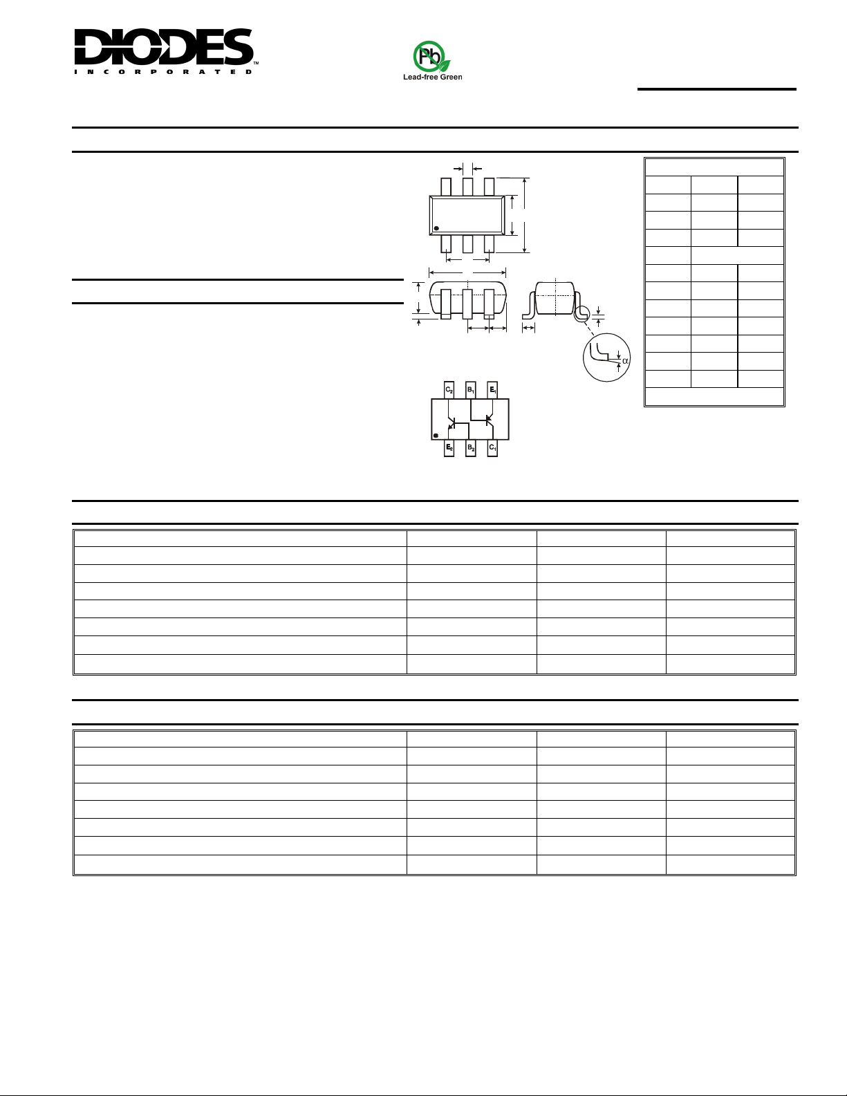
Mechanical Data
• Case: SOT-363
• Case Material: Molded Plastic. UL Flammability
Classification Rating 94V-0
• Moisture Sensitivity: Level 1 per J-STD-020C
• Terminals: Solderable per MIL-STD-202, Method 208
• Lead Free Plating (Matte Tin Finish annealed over Alloy 42
leadframe).
• Terminal Connections: See Diagram
• Marking Information: KNM, See Page 5
• Ordering & Date Code Information: See Page 5
• Weight: 0.006 grams (approximate)
A
B
1C2
2E2
G
H
K
J
E1, B1, C1 = PNP5401 Section
E2, B2, C2 = NPN5551 Section
D
E
1
C
B
C1B
L
F
MMDT5451
SOT-363
Dim Min Max
A 0.10 0.30
B 1.15 1.35
C 2.00 2.20
D 0.65 Nominal
F 0.30 0.40
M
H 1.80 2.20
J — 0.10
K 0.90 1.00
L 0.25 0.40
M 0.10 0.25
α
All Dimens mm ions in
0° 8°
Maximum Ratings, NPN 5551 Section @T
= 25°C unless otherwise specified
A
Characteristic Symbol NPN5551 Unit
Collector-Base Voltage
Collector-Emitter Voltage
Emitter-Base Voltage
Collector Current - Continuous (Note 1)
Power Dissipation (Note 1, 2)
Thermal Resistance, Junction to Ambient (Note 1)
Operating and Storage Temperature Range
V
V
V
R
Tj, T
CBO
CEO
EBO
IC
Pd
θ
JA
STG
180 V
160 V
6.0 V
200 mA
200 mW
625
-55 to +150
°C/W
°C
Maximum Ratings, PNP 5401 Section @T
= 25°C unless otherwise specified
A
Characteristic Symbol PNP5401 Unit
Collector-Base Voltage
Collector-Emitter Voltage
Emitter-Base Voltage
Collector Current – Continuous (Note 1)
Power Dissipation (Note 1, 2)
Thermal Resistance, Junction to Ambient (Note 1)
Operating and Storage Temperature Range
Notes: 1. Device mounted on FR-4 PCB, 1 inch x 0.85 inch x 0.062 inch; pad layout as shown on Diodes Inc. suggested pad layout document AP02001, which
can be found on our website at http://www.diodes.com/datasheets/ap02001.pdf.
2. Maximum combined dissipation.
3. No purposefully added lead.
4. Diodes Inc.'s "Green" policy can be found on our website at http://www.diodes.com/products/lead_free/index.php.
5. Product manufactured with Date Code UO (week 40, 2007) and newer are built with Green Molding Compound. Product manufactured prior to Date
Code UO are built with Non-Green Molding Compound and may contain Halogens or Sb2O3 Fire Retardants.
DS30171 Rev. 9 - 2
www.diodes.com
1 of 5
V
V
V
R
Tj, T
CBO
CEO
EBO
IC
Pd
θ
JA
STG
-160 V
-150 V
-5.0 V
-200 mA
200 mW
625 K/W
-55 to +150
°C
MMDT5451
© Diodes Incorporated
Page 2
Electrical Characteristics, NPN 5551 Section @T
Characteristic Symbol Min Max Unit Test Condition
OFF CHARACTERISTICS (Note 6)
Collector-Base Breakdown Voltage
Collector-Emitter Breakdown Voltage
Emitter-Base Breakdown Voltage
Collector Cutoff Current
Emitter Cutoff Current
ON CHARACTERISTICS (Note 6)
DC Current Gain
Collector-Emitter Saturation Voltage
Base-Emitter Saturation Voltage
SMALL SIGNAL CHARACTERISTICS
Output Capacitance
Small Signal Current Gain
Current Gain-Bandwidth Product
Noise Figure NF
V
(BR)CBO
V
(BR)CEO
V
(BR)EBO
I
CBO
I
EBO
hFE
V
CE(SAT)
V
BE(SAT)
C
hfe
⎯
obo
fT
= 25°C unless otherwise specified
A
180
160
6.0
⎯
80
80
30
⎯
⎯
⎯
50 250
⎯
⎯
⎯
50
50 nA
⎯
250
⎯
0.15
0.20
1.0 V
6.0 pF
V
V
V
nA
μA
⎯
V
⎯
100 300 MHz
⎯
8.0 dB
IC = 100μA, IE = 0
IC = 1.0mA, IB = 0
IE = 10μA, IC = 0
VCB = 120V, IE = 0
VCB = 120V, IE = 0, TA = 100°C
V
= 4.0V, IC = 0
EB
IC = 1.0mA, VCE = 5.0V
IC = 10mA, VCE = 5.0V
IC = 50mA, V
CE
= 5.0V
IC = 10mA, IB = 1.0mA
IC = 50mA, IB = 5.0mA
IC = 10mA, IB = 1.0mA
IC = 50mA, IB = 5.0mA
VCB = 10V, f = 1.0MHz, IE = 0
V
= 10V, IC = 1.0mA,
CE
f = 1.0kHz
VCE = 10V, IC = 10mA,
f = 100MHz
V
= 5.0V, IC = 200μA,
CE
RS = 1.0kΩ, f = 1.0kHz
Electrical Characteristics, PNP 5401 Section @T
Characteristic Symbol Min Max Unit Test Condition
OFF CHARACTERISTICS (Note 6)
Collector-Base Breakdown Voltage
Collector-Emitter Breakdown Voltage
Emitter-Base Breakdown Voltage
Collector Cutoff Current
Emitter Cutoff Current
V
(BR)CBO
V
(BR)CEO
V
(BR)EBO
I
CBO
I
EBO
⎯
ON CHARACTERISTICS (Note 6)
DC Current Gain
Collector-Emitter Saturation Voltage
Base-Emitter Saturation Voltage
hFE
V
CE(SAT)
V
BE(SAT)
SMALL SIGNAL CHARACTERISTICS
Output Capacitance
Small Signal Current Gain
Current Gain-Bandwidth Product
C
obo
hfe
fT
Noise Figure NF
Notes: 6. Short duration pulse test used to minimize self-heating effect.
DS30171 Rev. 9 - 2
2 of 5
www.diodes.com
= 25°C unless otherwise specified
A
-160
-150
-5.0
⎯
50
60
50
⎯
⎯
⎯
40 200
⎯
⎯
⎯
-50
-50 nA
⎯
240
⎯
-0.2
-0.5
-1.0 V
6.0 pF
V
V
V
nA
μA
⎯
V
⎯
100 300 MHz
⎯
8.0 dB
IC = -100μA, IE = 0
IC = -1.0mA, IB = 0
IE = -10μA, IC = 0
VCB = -120V, IE = 0
VCB = -120V, IE = 0, TA = 100°C
V
= -3.0V, IC = 0
EB
IC = -1.0mA, VCE = -5.0V
IC = -10mA, VCE = -5.0V
IC = -50mA, V
= -5.0V
CE
IC = -10mA, IB = -1.0mA
IC = -50mA, IB = -5.0mA
IC = -10mA, IB = -1.0mA
IC = -50mA, IB = -5.0mA
VCB = -10V, f = 1.0MHz, IE = 0
V
= -10V, IC = -1.0mA,
CE
f = 1.0kHz
VCE = -10V, IC = -10mA,
f = 100MHz
V
= -5.0V, IC = -200μA,
CE
RS = 10Ω, f = 1.0kHz
MMDT5451
© Diodes Incorporated
Page 3

C
O
CTO
R
T
O
T
TER
P, P
OWER
PATIO
T
TER VOLTAG
C CUR
RENT G
G
T
H
P
R
ODUCT
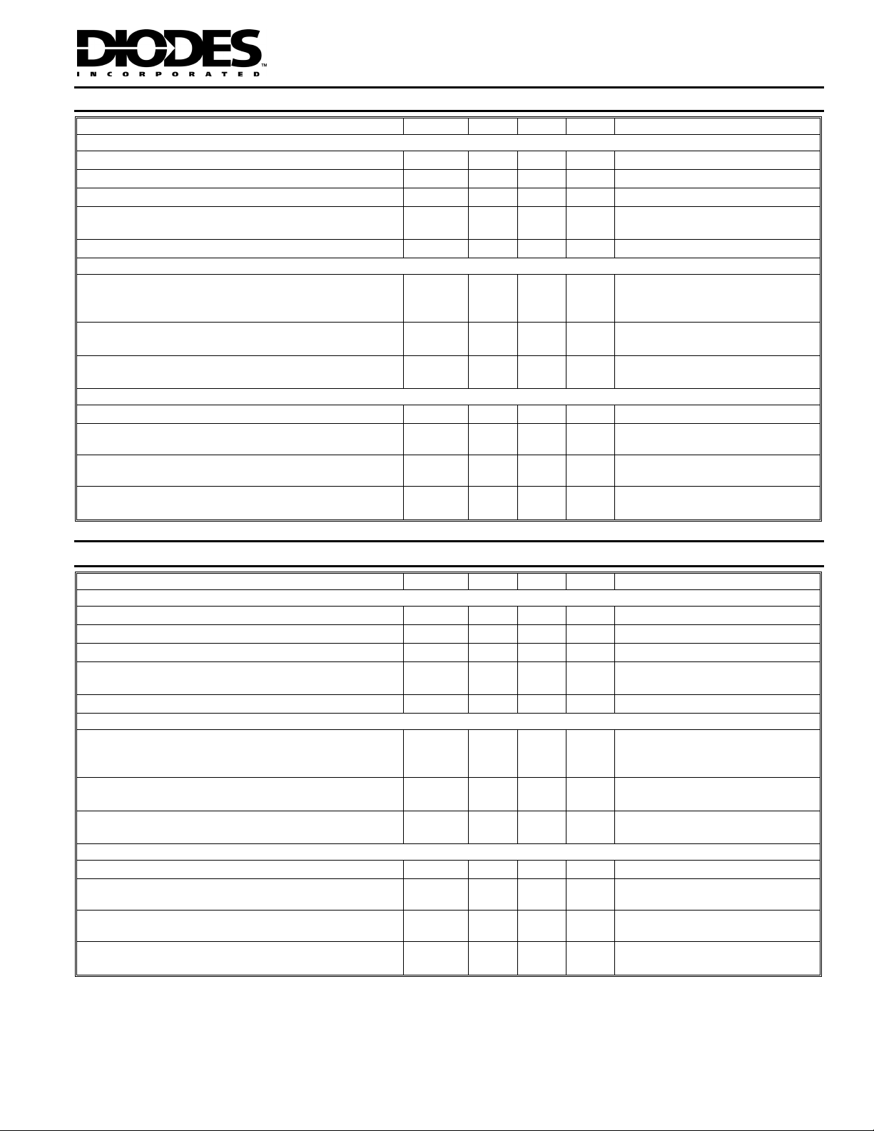
H
200
150
N (mW)
100
DISSI
50
D
0
0
25 50
T , AMBIENT TEMPERATURE (°C)
A
75
100 125
150
175
200
Fig. 1, Max Power Dissipation vs.
1,000
Ambient Temperature (Total Device)
V = 5V
CE
T = 150°C
A
AIN
100
T = 25°C
FE
h, D
A
10
T = -50°C
A
0.15
0.14
0.13
0.12
EMI
0.11
0.10
0.09
LLE
0.08
0.07
SATURATION VOLTAGE (V)
CE(SAT)
0.06
V,
0.05
0.04
1.0
0.9
E (V)
0.8
0.7
0.6
0.5
0.4
BE(ON)
V , BASE EMI
0.3
I
C
= 10
I
B
T = 150°C
A
T = -50°C
A
1
10 100
I , COLLECTOR CURRENT (mA)
C
Fig. 2, Collector Emitter Saturation Voltage
vs. Collector Current (NPN5551)
V = 5V
CE
T = -50°C
A
T = 25°C
A
T = 150°C
A
T = 25°C
A
1,000
1
1
I , COLLECTOR CURRENT (mA)
C
10
Fig. 3, DC Current Gain vs.
Collector Current (NPN5551)
1,000
z)
(M
100
10
AIN BANDWID
T
f,
1
110
I , COLLECTOR CURRENT (mA)
C
Fig. 5, Gain Bandwidth Product vs.
Collector Current (NPN5551)
100
100
0.2
0.1
110
I , COLLECTOR CURRENT (mA)
C
100
Fig. 4, Base Emitter Voltage
10.0
vs. Collector Current (NPN5551)
I
C
= 10
I
B
1.0
T = 150°C
A
0.1
SATURATION VOLTAGE (V)
CE(SAT)
V , COLLECTOR TO EMITTER
T = 25°C
A
T = -50°C
A
0.01
1
10 100
I , COLLECTOR CURRENT (mA)
C
1,000
Fig. 6, Collector Emitter Saturation Voltage
vs. Collector Current (PNP5401)
DS30171 Rev. 9 - 2
3 of 5
www.diodes.com
MMDT5451
© Diodes Incorporated
Page 4

T
TER VOLTAG
G
T
H PRODUCT
H
10,000
1,000
1.0
V = 5V
CE
0.9
E (V)
0.8
T = -50°C
A
0.7
100
FE
10
h , DC CURRENT GAIN
1
110100
I , COLLECTOR CURRENT (mA)
C
Fig. 7, DC Current Gain vs. Collector Current (PNP5401)
1,000
V = 10V
CE
z)
(M
100
10
1,000
0.6
T = 25°C
A
0.5
0.4
T = 150°C
A
0.3
BE(ON )
V , BASE EMI
0.2
0.1
0.1 1.0 10 100
I , COLLECTOR CURRENT (mA)
C
Fig. 8, Base Emitter Voltage
vs. Collector Current (PNP5401)
AIN BANDWID
t
f,
1
1
I , COLLECTOR CURRENT (mA)
C
10
100
Fig. 9, Gain Bandwidth Product
vs. Collector Current (PNP5401)
DS30171 Rev. 9 - 2
4 of 5
www.diodes.com
MMDT5451
© Diodes Incorporated
Page 5

Ordering Information (Note 7)
Device
MMDT5451-7-F SOT-363 3000/Tape & Reel
Notes: 7. For packaging details, go to our website at http://www.diodes.com/datasheets/ap02007.pdf.
Packaging Shipping
Marking Information
KNM = Product Type Marking Code
KNM
Date Code Key
Year 1998 1999 2000 2001 2002 2003 2004 2005 2006 2007 2008 2009 2010 2011 2012
Code J K L M N P R S T U V W X Y Z
Month
Code
Diodes Incorporated and its subsidiaries reserve the right to make modifications, enhancements, improvements, corrections or other changes
without further notice to any product herein. Diodes Incorporated does not assume any liability arising out of the application or use of any product
described herein; neither does it convey any license under its patent rights, nor the rights of others. The user of products in such applications shall
assume all risks of such use and will agree to hold Diodes Incorporated and all the companies whose products are represented on our website,
harmless against all damages.
Diodes Incorporated products are not authorized for use as critical components in life support devices or systems without the expressed written
approval of the President of Diodes Incorporated.
Jan Feb Mar Apr May Jun Jul Aug Sep Oct Nov Dec
1 2 3 4 5 6 7 8 9 O N D
YM = Date Code Marking
Y = Year ex: N = 2002
YM
M = Month ex: 9 = September
IMPORTANT NOTICE
LIFE SUPPORT
DS30171 Rev. 9 - 2
5 of 5
www.diodes.com
MMDT5451
© Diodes Incorporated
 Loading...