

Page 1
Features
• Complementary Pair: One 3904 (NPN) and One 3906 (PNP)
• Epitaxial Planar Die Construction
• Ideally Suited for Automated Assembly Processes
• Lead Free by Design/RoHS Compliant (Note 1)
• “Green” Device (Note 2)
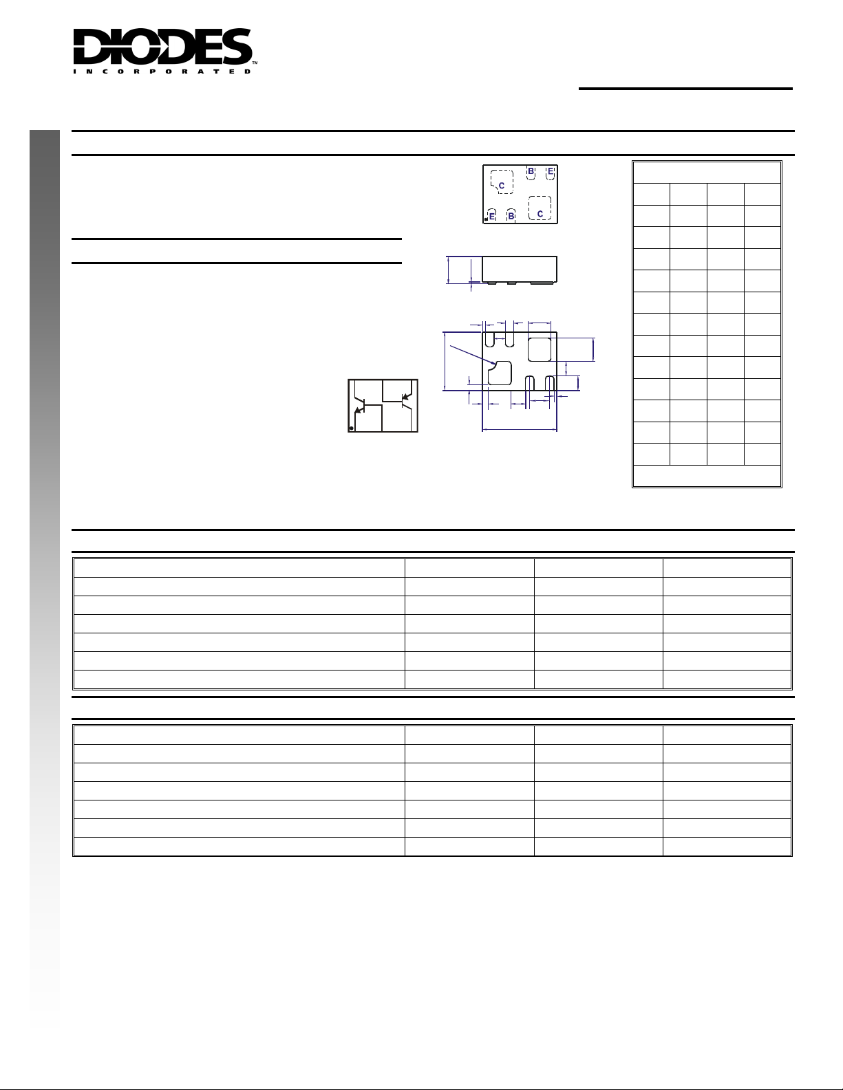
Mechanical Data
• Case: DFN1310H4-6
• Case Material: Molded Plastic. “Green Molding”
Compound. UL Flammability Classification Rating 94V-0
• Moisture Sensitivity: Level 1 per J-STD-020C
• Terminals: Finish – NiPdAu over Copper leadframe (Lead
NEW PRODUCT
Free Plating) Solderable per MIL-STD-202, Method 208
• Marking & Type Code Information: See Page 4
• Ordering Information: See Page 4
MMDT3946LP4
COMPLEMENTARY NPN / PNP SURFACE MOUNT TRANSISTORS
DFN1310H4-6
Dim Min Max Typ
A 1.25 1.38 1.30
B 0.95 1.08 1.00
C 0.20 0.30 0.25
D* - - 0.10
E** - - 0.20
G - 0.40 -
H 0 0.05 0.02
K* 0.10 0.20 0.15
L* 0.30 0.50 0.40
M** - - 0.35
N* - - 0.25
Z** - - 0.05
All Dimensions in mm
* Dimensions D, K, L, N Repeat 4X
** Dimensions E, M, Z Repeat 2X
B
C
2
E
2
E
1
1
B
C
2
1
Internal Schematic
(TOP VIEW)
E1, B1, C1 = PNP3906 Section
E
2
Top View
G
H
Side View
K
Z
R
0
.
1
5
0
B
D
L
E
M
ND
A
Bottom View
, B2, C2 = NPN3904 Section
L
N
C
Z
Maximum Ratings, NPN 3904 Section @T
= 25°C unless otherwise specified
A
Characteristic Symbol Value Unit
Collector-Base Voltage
Collector-Emitter Voltage
Emitter-Base Voltage
Collector Current – Continuous
Power Dissipation (Notes 3, 4)
Thermal Resistance, Junction to Ambient (Note 3)
Maximum Ratings, PNP 3906 Section @T
V
CBO
V
CEO
V
EBO
I
C
P
d
R
JA
θ
= 25°C unless otherwise specified
A
60 V
40 V
6.0 V
200 mA
200 mW
625 °C/W
Characteristic Symbol Value Unit
Collector-Base Voltage
Collector-Emitter Voltage
Emitter-Base Voltage
Collector Current - Continuous (Note 1)
Power Dissipation (Notes 3, 4)
Thermal Resistance, Junction to Ambient (Note 3)
V
CBO
V
CEO
V
EBO
I
C
P
d
R
JA
θ
-40 V
-40 V
-5.0 V
-200 mA
200 mW
625 °C/W
Notes: 1. No purposefully added lead.
2. Diodes Inc.’s “Green” policy can be found on our website at http://www.diodes.com/products/lead_free/index.php.
3. Device mounted on FR-4 PCB.
4. Maximum combined dissipation.
DS30822 Rev. 4 - 2
1 of 5
www.diodes.com
MMDT3946LP
© Diodes Incorporated
Page 2
Electrical Characteristics, NPN 3904 Section @T
OFF CHARACTERISTICS (Note 5)
Collector-Base Breakdown Voltage
Collector-Emitter Breakdown Voltage
Emitter-Base Breakdown Voltage
Collector Cutoff Current
Base Cutoff Current
ON CHARACTERISTICS (Note 5)
DC Current Gain
Collector-Emitter Saturation Voltage
NEW PRODUCT
Base-Emitter Saturation Voltage
SMALL SIGNAL CHARACTERISTICS
Output Capacitance
Current Gain-Bandwidth Product
SWITCHING CHARACTERISTICS
Delay Time
Rise Time
Storage Time
Fall Time
Characteristic Symbol Min Max Unit Test Condition
V
(BR)CBO
V
(BR)CEO
V
(BR)EBO
I
CEX
I
BL
h
FE
V
CE(SAT)
V
BE(SAT)
C
obo
f
T
t
d
t
r
t
s
t
f
60
40
6.0
⎯
⎯
40
70
100
60
30
⎯
0.65
⎯
⎯
300
⎯
⎯
⎯
⎯
= 25°C unless otherwise specified
A
⎯
⎯
⎯
50 nA
50 nA
⎯
⎯
300
⎯
⎯
0.20
0.30
0.85
0.95
4.0 pF
⎯
35 ns
35 ns
200 ns
50 ns
V
V
V
⎯
V
V
MHz
I
= 10μA, IE = 0
C
I
= 1.0mA, IB = 0
C
I
= 10μA, IC = 0
E
V
= 30V, V
CE
V
= 30V, V
CE
= 100µA, V
I
C
I
= 1.0mA, VCE = 1.0V
C
= 10mA, VCE = 1.0V
I
C
I
= 50mA, V
C
= 100mA, VCE = 1.0V
I
C
EB(OFF)
EB(OFF)
CE
= 1.0V
CE
= 3.0V
= 3.0V
= 1.0V
IC = 10mA, IB = 1.0mA
I
= 50mA, IB = 5.0mA
C
= 10mA, IB = 1.0mA
I
C
= 50mA, IB = 5.0mA
I
C
V
= 5.0V, f = 1.0MHz, IE = 0
CB
= 20V, IC = 20mA,
V
CE
f = 100MHz
= 3.0V, IC = 10mA,
V
CC
V
= -0.5V, IB1 = 1.0mA
BE(off)
= 3.0V, IC = 10mA,
V
CC
I
= IB2 = 1.0mA
B1
Electrical Characteristics, PNP 3906 Section @T
Characteristic Symbol Min Max Unit Test Condition
OFF CHARACTERISTICS (Note 5)
Collector-Base Breakdown Voltage
Collector-Emitter Breakdown Voltage
Emitter-Base Breakdown Voltage
Collector Cutoff Current
Base Cutoff Current
V
(BR)CBO
V
(BR)CEO
V
(BR)EBO
I
CEX
I
BL
ON CHARACTERISTICS (Note 5)
DC Current Gain
Collector-Emitter Saturation Voltage
Base-Emitter Saturation Voltage
h
V
CE(SAT)
V
BE(SAT)
FE
SMALL SIGNAL CHARACTERISTICS
Output Capacitance
Current Gain-Bandwidth Product
C
obo
f
T
SWITCHING CHARACTERISTICS
Delay Time
Rise Time
Storage Time
Fall Time
Notes: 5. Short duration test pulse used to minimize self-heating effect.
t
d
t
r
t
s
t
f
-40
-40
-5.0
⎯
⎯
60
80
100
60
30
⎯
-0.65
⎯
⎯
250
⎯
⎯
⎯
⎯
= 25°C unless otherwise specified
A
⎯
⎯
⎯
-50 nA
-50 nA
⎯
⎯
300
⎯
⎯
-0.25
-0.40
-0.85
-0.95
4.5 pF
⎯
35 ns
35 ns
225 ns
75 ns
V
V
V
⎯
V
V
MHz
I
= -10μA, IE = 0
C
I
= -1.0mA, IB = 0
C
I
= -10μA, IC = 0
E
V
CE
V
CE
= -100µA, V
I
C
= -1.0mA, VCE = -1.0V
I
C
I
= -10mA, VCE = -1.0V
C
= -50mA, V
I
C
I
= -100mA, VCE = -1.0V
C
= -10mA, IB = -1.0mA
I
C
= -50mA, IB = -5.0mA
I
C
= -10mA, IB = -1.0mA
I
C
I
= -50mA, IB = -5.0mA
C
V
CB
V
CE
f = 100MHz
V
CC
V
BE(off)
V
CC
I
B1
= -30V, V
= -30V, V
EB(OFF)
EB(OFF)
= -1.0V
CE
= -1.0V
CE
= -3.0V
= -3.0V
= -5.0V, f = 1.0MHz, IE = 0
= -20V, IC = -10mA,
= -3.0V, IC = -10mA,
= 0.5V, IB1 = -1.0mA
= -3.0V, IC = -10mA,
= IB2 = -1.0mA
DS30822 Rev. 4 - 2
2 of 5
www.diodes.com
MMDT3946LP
© Diodes Incorporated
Page 3

P, P
OWER
P
T
O
N
C CUR
REN
T GAIN
C
O
CTO
R
T
TER
T
T
R
TURAT
O
OLTAG
250
NEW PRODUCT
200
(mW)
I
A
150
DISS I
100
D
1,000
100
50
0
0
25 50
T , AMBIENT TEMPERATURE (°C)
A
75 100 125
Fig. 1, Max Power Dissipation vs
Ambient Temperat ure (Total Device) (N ot e 3)
T = 125°C
A
T = +25°C
T = -25°C
A
A
150
175
200
f = 1MHz
Fig. 2, Typical Output Capacitance
Characteristics (NPN-3904)
1
I
C
(V)
= 10
I
B
-EMI
0.1
FE
h, D
E (V)
N V
I
SA
E
10
10
1
0.1
1
1
I , COLLECTOR CURRENT (mA)
C
10
100
Fig. 3, Typical DC Current Gain vs
Collector Current (NPN-3904)
I
C
= 10
I
B
V = 1.0V
CE
1,000
LLE
CE(SAT)
V,
SATURATION VOLTA GE
0.01
0.1 1 10
I , COLLECTOR CURRENT (mA)
C
100
1,000
Fig. 4, Typical Collector-Emitter
Saturation Voltage vs. Collector Current (NPN-3904)
f = 1MHz
0.1
0.1 1 10
BE(SAT)
V , BASE-EMI
I , COLLECTOR CURRENT (mA)
C
100
Fig. 5, Typical Base-Emitter
Saturation Voltage vs. Collector Current (NPN-3904)
DS30822 Rev. 4 - 2
1,000
3 of 5
www.diodes.com
Fig. 6, Typical Output Capacitance
Characteristics (PNP-3906)
MMDT3946LP
© Diodes Incorporated
Page 4

C CUR
R
T
G
C
O
CTO
R
T
TER
1,000
10
NEW PRODUCT
AIN
100
EN
FE
h, D
10
1
0.1
T = 125°C
A
T = +25°C
T = -25°C
A
1
I , COLLECTOR CURRENT (mA)
C
A
10
Fig. 7, Typical DC Current Gain vs
Collector Current (PNP-3906)
I
C
= 10
I
B
100
V = 1.0V
CE
1,000
-EMI
I
C
= 10
I
B
1
LLE
0.1
SATURATION VOLTAGE (V)
CE(SAT)
V,
0.01
1
10
I , COLLECTOR CURRENT (mA)
C
100
1,000
Fig. 8, Typical Collector-Emitter Saturation Voltage
vs. Collector Current (PNP-3906)
BE(SAT)
V , BASE-EMITTER SATURA TION VOLTAGE (V)
I , COLLECTOR CURRENT (mA)
C
Fig. 9, Typical Base-Emitter Saturation Voltage
vs. Collector Current ( PNP-390 6)
Ordering Information (Note 6)
Device
MMDT3946LP4-7 DFN1310H4-6 3000/Tape & Reel
Notes: 6. For packaging details, go to our website at http://www.diodes.com/datasheets/ap02007.pdf.
Packaging Shipping
Marking Information
46= Product Type Marking Code
DS30822 Rev. 4 - 2
46
www.diodes.com
4 of 5
MMDT3946LP
© Diodes Incorporated
Page 5

Diodes Incorporated and its subsidiaries reserve the right to make modifications, enhancements, improvements, corrections or other changes
without further notice to any product herein. Diodes Incorporated does not assume any liability arising out of the application or use of any product
described herein; neither does it convey any license under its patent rights, nor the rights of others. The user of products in such applications shall
assume all risks of such use and will agree to hold Diodes Incorporated and all the companies whose products are represented on our website,
harmless against all damages.
Diodes Incorporated products are not authorized for use as critical components in life support devices or systems without the expressed written
approval of the President of Diodes Incorporated.
IMPORTANT NOTICE
LIFE SUPPORT
NEW PRODUCT
DS30822 Rev. 4 - 2
5 of 5
www.diodes.com
MMDT3946LP
© Diodes Incorporated
 Loading...