

Page 1
Lead-free Green
Features
A
M
J
L
D
F
B
C
H
K
C2B1E
1
E2B2C
1
C2B1E
1
E2B2C
1
MMDT2227M
COMPLEMENTARY NPN / PNP SMALL
SIGNAL SURFACE MOUNT TRANSISTOR
· Complementary Pair
· Epitaxial Planar Die Construction
· One 2222A Type (NPN),
One 2907A Type (PNP)
· Ideal for Low Power Amplification and Switching
· Lead Free By Design/RoHS Compliant (Note 2)
· "Green Device" (Note 3)
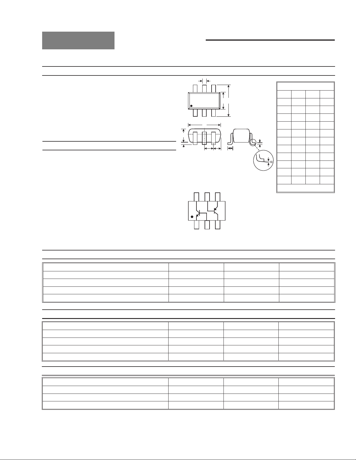
Mechanical Data
· Case: SOT-26
· Case Material: Molded Plastic, “Green” Molding
Compound. UL Flammability Classification Rating 94V-0
· Moisture Sensitivity: Level 1 per J-STD-020C
· Terminals: Finish - Matte Tin annealed over Copper
leadframe. Solderable per MIL-STD-202, Method 208
· Terminal Connections: See Diagram
· Ordering & Date Code Information: See Page 3
· Marking (See Page 3): K27
· Weight: 0.006 grams (approximate)
Note: E1, B1, and C1 = 2907A Type (PNP),
E2, B2, and C2 = 2222A Type (NPN).
Type marking indicates orientation.
SOT-26
Dim Min Max Typ
A
0.35 0.50 0.38
B
1.50 1.70 1.60
C
2.70 3.00 2.80
D
¾ ¾ 0.95
F
¾ ¾ 0.55
H
2.90 3.10 3.00
J
0.013 0.10 0.05
K
1.00 1.30 1.10
L
0.35 0.55 0.40
M
0.10 0.20 0.15
a
0° 8° ¾
All Dimensions in mm
Maximum Ratings, 2222A Type (NPN)
@ TA = 25°C unless otherwise specified
Characteristic Symbol 2222A (NPN) Unit
Collector-Base Voltage
Collector-Emitter Voltage
Emitter-Base Voltage
Collector Current - Continuous
Maximum Ratings, 2907A Type (PNP)
@ TA = 25°C unless otherwise specified
V
CBO
V
CEO
V
EBO
I
C
75 V
40 V
6.0 V
600 mA
Characteristic Symbol 2907A (PNP) Unit
Collector-Base Voltage
Collector-Emitter Voltage
Emitter-Base Voltage
Collector Current - Continuous
Maximum Ratings, Total
@ TA = 25°C unless otherwise specified
V
CBO
V
CEO
V
EBO
I
C
-60 V
-60 V
-5.0 V
-600 mA
Characteristic Symbol Value Unit
Total Power Dissipation (Note 1)
Thermal Resistance, Junction to Ambient (Note 1)
Operating and Storage Temperature Range
Note: 1. Device mounted on FR-4 PCB, 1 inch x 0.85 inch x 0.062 inch; pad layout as shown on Diodes Inc. suggested pad layout
document AP02001, which can be found on our website at http://www.diodes.com/datasheets/ap02001.pdf.
2. No purposefully added lead.
3. Diodes Inc.'s "Green" policy can be found on our website at http://www.diodes.com/products/lead_free/index.php.
DS30718 Rev. 4 - 2 1 of 4 MMDT2227M
R
Tj, T
P
qJA
d
STG
300
mW
417 °C/W
-55 to +150 °C
www.diodes.com ã Diodes Incorporated
Page 2
Electrical Characteristics, 2222A Type (NPN)
Characteristic Symbol Min Max Unit Test Condition
OFF CHARACTERISTICS (Note 4)
Collector-Base Breakdown Voltage
Collector-Emitter Breakdown Voltage
Emitter-Base Breakdown Voltage
Collector Cutoff Current
Collector Cutoff Current
Emitter Cutoff Current
Base Cutoff Current
ON CHARACTERISTICS (Note 4)
DC Current Gain
Collector-Emitter Saturation Voltage
Base-Emitter Saturation Voltage
SMALL SIGNAL CHARACTERISTICS
Output Capacitance
Input Capacitance
Current Gain-Bandwidth Product
SWITCHING CHARACTERISTICS
Delay Time
Rise Time
Storage Time
Fall Time
V
(BR)CBO
V
(BR)CEO
V
(BR)EBO
I
CBO
I
CEX
I
EBO
I
h
V
CE(SAT)
V
BE(SAT)
C
C
BL
obo
f
t
t
t
t
FE
ibo
T
d
r
s
f
@ TA = 25°C unless otherwise specified
75 ¾ V
40 ¾ V
6.0 ¾ V
¾ 10
¾ 10 nA
¾ 10 nA
¾ 20 nA
35
50
75
100
40
50
35
¾
0.6
¾
¾
¾
¾
300
¾
¾
¾
0.3
1.0
1.2
2.0
¾ 8 pF
— 25 pF
300 ¾ MHz
¾ 10 ns
¾ 25 ns
¾ 225 ns
¾ 60 ns
IC = 10mA, IE = 0
IC = 10mA, IB = 0
IE = 10mA, IC = 0
VCB = 60V, IE = 0
nA
VCB = 60V, IE = 0, TA = 150°C
mA
V
= 60V, V
CE
V
= 3.0V, IC = 0
EB
V
= 60V, V
CE
IC = 100mA, V
IC = 1.0mA, VCE = 10V
IC = 10mA, VCE = 10V
IC = 150mA, V
¾
IC = 500mA, VCE = 10V
IC = 10mA, VCE = 10V, TA = -55°C
IC = 150mA, VCE = 1.0V
IC = 150mA, IB = 15mA
V
IC = 500mA, IB = 50mA
IC = 150mA, IB = 15mA
V
IC = 500mA, IB = 50mA
VCB = 10V, f = 1.0MHz, IE = 0
VEB = 0.5V, f = 1.0MHz, IC = 0
VCE = 20V, IC = 20mA,
f = 100MHz
VCC = 30V, IC = 150mA,
V
BE(off)
VCC = 30V, IC = 150mA,
IB1 = IB2 = 15mA
= 3.0V
EB(OFF)
= 3.0V
EB(OFF)
= 10V
CE
= 10V
CE
= - 0.5V, IB1 = 15mA
Note: 4. Pulse test: Pulse width £ 300ms, duty cycle £ 2%.
DS30718 Rev. 4 - 2 2 of 4 MMDT2227M
www.diodes.com
Page 3

Electrical Characteristics, 2907A Type (PNP)
K27
YM
Characteristic Symbol Min Max Unit Test Condition
OFF CHARACTERISTICS (Note 5)
Collector-Base Breakdown Voltage
Collector-Emitter Breakdown Voltage
Emitter-Base Breakdown Voltage
Collector Cutoff Current
Collector Cutoff Current
Base Cutoff Current
ON CHARACTERISTICS (Note 5)
DC Current Gain
Collector-Emitter Saturation Voltage
Base-Emitter Saturation Voltage
SMALL SIGNAL CHARACTERISTICS
Output Capacitance
Input Capacitance
Current Gain-Bandwidth Product
SWITCHING CHARACTERISTICS
Turn-On Time
Delay Time
Rise Time
Turn-Off Time
Storage Time
Fall Time
V
(BR)CBO
V
(BR)CEO
V
(BR)EBO
I
CBO
I
CEX
I
h
V
CE(SAT)
V
BE(SAT)
C
C
t
t
BL
obo
f
on
t
t
off
t
t
FE
ibo
T
d
r
s
f
@ TA = 25°C unless otherwise specified
-60 ¾ V
-60 ¾ V
-5.0 ¾ V
¾ -10
¾ -50 nA
¾ -50 nA
75
100
100
100
50
¾
¾
¾
¾
¾
300
¾
-0.4
-1.6
-1.3
-2.6
¾ 8.0 pF
— 30 pF
200 ¾ MHz
IC = -10mA, IE = 0
IC = -10mA, IB = 0
IE = -10mA, IC = 0
VCB = -50V, IE = 0
nA
VCB = -50V, IE = 0, TA = 125°C
mA
V
= -30V, V
CE
V
= -30V, V
CE
IC = -100µA, V
IC = -1.0mA, VCE = -10V
IC = -10mA, VCE = -10V
¾
IC = -150mA, V
IC = -500mA, VCE = -10V
IC = -150mA, IB = -15mA
V
IC = -500mA, IB = -50mA
IC = 150mA, IB = 15mA
V
IC = 500mA, IB = 50mA
VCB = -10V, f = 1.0MHz, IE = 0
VEB = -2.0V, f = 1.0MHz, IC = 0
VCE = -20V, IC = -50mA,
f = 100MHz
¾ 45 ns
¾ 10 ns
VCC = -30V, IC = -150mA,
IB1 = -15mA
¾ 40 ns
¾ 100 ns
¾ 80 ns
VCC = -6.0V, IC = -150mA,
IB1 = IB2 = -15mA
¾ 30 ns
EB(OFF)
EB(OFF)
= -10V
CE
= -10V
CE
= -0.5V
= -0.5V
Note: 5. Short duration pulse test used to minimize self-heating effect.
Ordering Information
Device
MMDT2227M-7
Note: 6. For Packaging Details, go to our website at http://www.diodes.com/datasheets/ap02007.pdf.
(Note 6)
Packaging Shipping
SOT-26 3000/Tape & Reel
Marking Information
K27 = Product Type Marking Code
YM = Date Code Marking
Y = Year ex: S = 2005
M = Month ex: 9 = September
Date Code Key
Year 2005
Code S
Month Jan Feb March Apr May Jun Jul
Code
1 2 3 4 5 6 7
2006 2007 2008 2009
T U V W
2010 2011 2012
X Y Z
Aug Sep Oct Nov Dec
8 9 O N D
DS30718 Rev. 4 - 2 3 of 4 MMDT2227M
www.diodes.com
Page 4

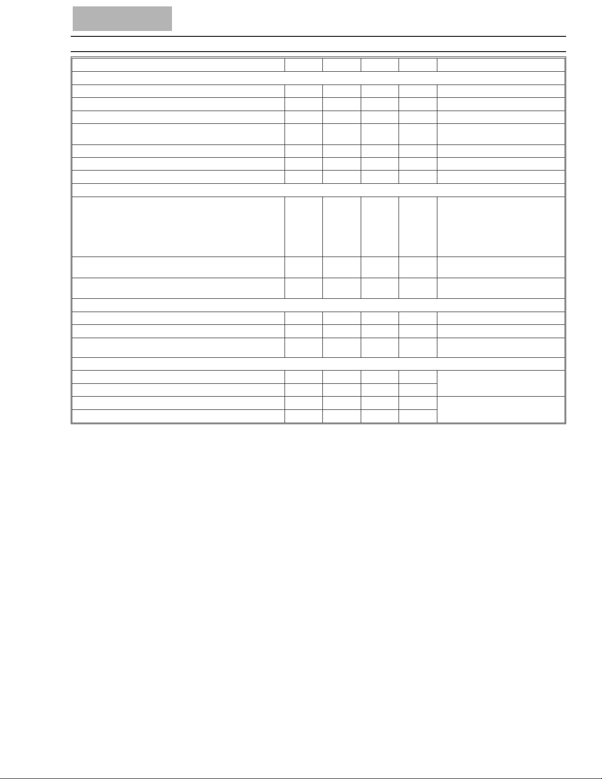
1.0
10
0.1
10
1.0
50
CAPACITANCE (pF)
V , REVERSE VOLTS (V)
R
Fig. 1 (2222A) Typical Capacitance
Cobo
100
Cibo
0.001
0.01
1
10
0.1
100
0
0.2
0.4
0.6
0.8
1.0
1.2
1.4
1.6
1.8
2.0
I BASE CURRENT (mA)
B,
Fig. 2 (2222A) Typical Collector Saturation Region
V COLLECTOR-EMITTER VOLTAGE (V)
CE
I = 1mA
C
I = 10mA
C
I = 30mA
C
I = 100mA
C
I = 300mA
C
1
10
100
0.1 1 10 100
CAPACITANCE (pF)
V , REVERSE VOLTS (V)
R
Fig. 3 (2907A) Typical Capacitance
Cibo
Cobo
I BASE CURRENT (mA)
B,
Fig. 4 (2907A) Typical Collector Saturation Region
V COLLECTOR-EMITTER VOLTAGE (V)
CE
-0.2
0
-0.4
-0.6
-0.8
-1.0
-1.2
-1.4
-1.6
-0.01
-0.001
-1
-10
-0.1
-100
I = -1mA
C
I = -10mA
C
I = -30mA
C
I = -100mA
C
I = -300mA
C
IMPORTANT NOTICE
Diodes Incorporated and its subsidiaries reserve the right to make modifications, enhancements, improvements, corrections or other changes without further
notice to any product herein. Diodes Incorporated does not assume any liability arising out of the application or use of any product described herein; neither
does it convey any license under its patent rights, nor the rights of others. The user of products in such applications shall assume all risks of such use and will
agree to hold Diodes Incorporated and all the companies whose products are represented on our website, harmless against all damages.
LIFE SUPPORT
Diodes Incorporated products are not authorized for use as critical components in life support devices or systems without the expressed written approval of the
President of Diodes Incorporated.
DS30718 Rev. 4 - 2 4 of 4 MMDT2227M
www.diodes.com
 Loading...