

Page 1
MBR20100C
Document number: DS36950 Rev. 2 - 2
1 of 13
www.diodes.com
April 2014
© Diodes Incorporated
MBR20100C
Product Summary
V
RRM
(V)
IO (A)
VF
(MAX)
(V)
@ +25°C
IR
(MAX)
(mA)
@ +25°C
100V
2x10A
0.85
0.1
Description
High voltage dual Schottky rectifier suited for switch mode power
supplies and other power converters. This device is intended for use
in medium voltage operation, and particularly, in high frequency
circuits where low switching losses and low noise are required.
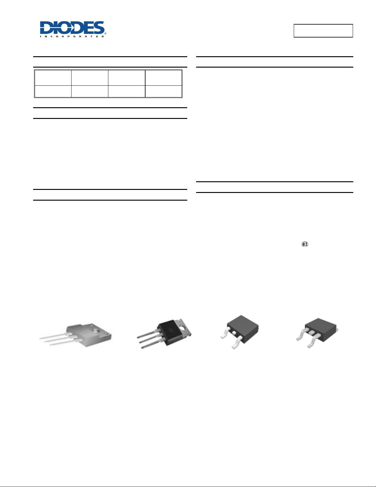
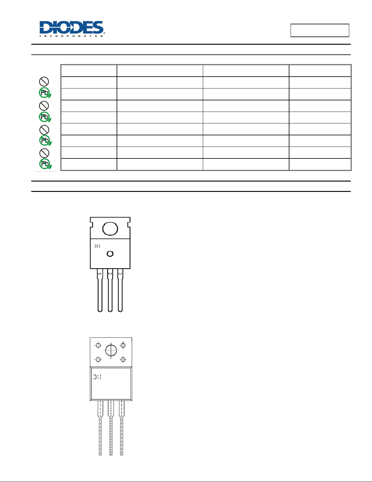
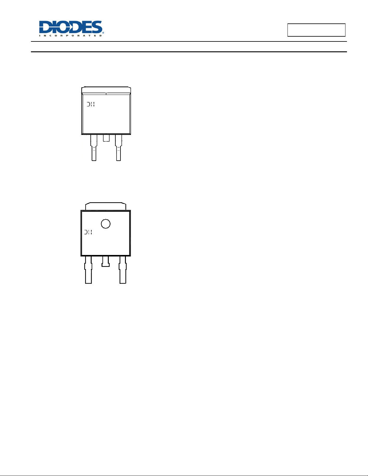
The MBR20100C is available in standard TO-220-3 (2), TO-220F-3
(Option 1), TO-252-2 (1) and TO-263-2 packages.
Applications
Power Supply Output Rectification
Power Management
Instrumentation
Features
Low Forward Voltage: 0.85V @ +25oC
High Surge Current Capability
+150oC Operating Junction Temperature
20A Total (10A Each Diode Leg)
Guard-Ring for Stress Protection
Pb-free Package
TO-220-3 (2), TO-220F-3 (Option 1), TO-252-2 (1) and TO-263-2
Lead-Free Finish; RoHS Compliant (Notes 1 & 2)
Available in “Green” Packages: TO-220-3 (2), TO-220F-3 (Option
1), TO-252-2 (1) and TO-263-2
Lead-Free Finish; RoHS Compliant (Notes 1 & 2)
Halogen and Antimony Free. “Green” Device (Note 3)
Mechanical Data
Case: TO-220-3 (2), TO-220F-3 (Option 1), TO-252-2 (1) and TO-
263-2
Case Material: Molded Plastic, “Green” Molding Compound. UL
Flammability Classification Rating 94V-0
Terminals: Finish - Matte Tin Annealed over Copper Leadframe.
Solderable per MIL-STD-202, Method 208
Polarity: See Below
Weight
TO-220-3 (2), TO-220F-3 (Option 1) and TO-263-2 ─ 1.9
Grams (Approximate)
TO-252-2 (1) ─ 0.31Grams (Approximate)
HIGH VOLTAGE POWER SCHOTTKY RECTIFIER
TO-220F-3 (Option 1) TO-220-3 (2) TO-252-2 (1) TO-263-2
Notes: 1. EU Directive 2002/95/EC (RoHS) & 2011/65/EU (RoHS 2) compliant. All applicable RoHS exemptions applied.
2. See http://www.diodes.com/quality/lead_free.html for more information about Diodes Incorporated’s definitions of Halogen- and Antimony-free, "Green"
and Lead-free.
3. Halogen- and Antimony-free "Green” products are defined as those which contain <900ppm bromine, <900ppm chlorine (<1500ppm total Br + Cl) and
<1000ppm antimony compounds.
Page 2
MBR20100C
Document number: DS36950 Rev. 2 - 2
2 of 13
www.diodes.com
April 2014
© Diodes Incorporated
MBR20100C
Green Green
MBR20100C XX XX - XX
PackingPackageProduct Name
Blank : Tube
T : TO-220-3 (2)
E1/G1
E1 : Lead Free
G1 : Green
TF : TO-220F-3
(Option 1)
D : TO-252-2 (1)
S2 : TO-263-2
TR : Tape & Reel
Package
Part Number
Marking ID
Packing
TO-220-3 (2)
MBR20100CT-E1 (Note 5)
MBR20100CT-E1
50 Pieces/Tube
TO-220-3 (2)
MBR20100CT-G1 (Note 6)
MBR20100CT-G1
50 Pieces/Tube
TO-220F-3 (Option 1)
MBR20100CTF-E1 (Note 5)
MBR20100CTF-E1
50 Pieces/Tube
TO-220F-3 (Option 1)
MBR20100CTF-G1 (Note 6)
MBR20100CTF-G1
50 Pieces/Tube
Pb
1
2
3
A1
K
A2
1
2
3
A1
K
A2
A1
A2
K
1
2
3
A2
K
A1
A1
A2
1
2
3
K
Pb
Pin Assignments
(Front View) (Front View) (Top View)
TO-220-3 (2) TO-220F-3 (Option 1) TO-263-2
(Top View)
TO-252-2 (1) Internal Structure of MBR20100C
Ordering Information (Note 4)
Notes: 4. For packaging details, go to our website at http://www.diodes.com/products/packages.html.
5. Diodes IC's Pb-free products, as designated with "E1" suffix in the part number, are RoHS compliant. Not recommended for new design.
6. Products with "G1" suffix are available in green packages. Recommended MBR(F)20100CT-LJ for new design, MBR(F)20100CT-LJ can replace the
“MBR20100CT-G1 and MBR20100CTF-G1” products.
Page 3
MBR20100C
Document number: DS36950 Rev. 2 - 2
3 of 13
www.diodes.com
April 2014
© Diodes Incorporated
MBR20100C
Package
Part Number
Marking ID
Packing
TO-252-2 (1)
MBR20100CD-E1 (Note 5)
MBR20100CD-E1
100 Pieces/Tube
TO-252-2 (1)
MBR20100CD-G1
MBR20100CD-G1
100 Pieces/Tube
TO-252-2 (1)
MBR20100CDTR-E1 (Note 5)
MBR20100CD-E1
2500 Pieces/Tape & Reel
TO-252-2 (1)
MBR20100CDTR-G1
MBR20100CD-G1
2500 Pieces/Tape & Reel
TO-263-2
MBR20100CS2-E1 (Note 5)
MBR20100CS2-E1
50 Pieces/Tube
TO-263-2
MBR20100CS2-G1
MBR20100CS2-G1
50 Pieces/Tube
TO-263-2
MBR20100CS2TR-E1 (Note 5)
MBR20100CS2-E1
800 Pieces/Tape & Reel
TO-263-2
MBR20100CS2TR-G1
MBR20100CS2-G1
800 Pieces/Tape & Reel
XXXXXXXX
XX-XX
YWWAXX
Green Green Green Green
PbPbPb
First and Second Lines: Logo and Marking ID
(See Ordering Information)
Third Line: Date Code
Y: Year
WW: Work Week of Molding
A: Assembly House Code
XX: 7th and 8th Digits of Batch Number
XXXXXXXX
XXX-XX
YWWAXX
First and Second Lines: Logo and Marking ID
(See Ordering Information)
Third Line: Date Code
Y: Year
WW: Work Week of Molding
A: Assembly House Code
XX: 7th and 8th Digits of Batch Number
Pb
Ordering Information (Cont. Note 4)
Marking Information
(1) TO-220-3 (2)
(Front View)
(2) TO-220F-3 (Option 1)
(Front View)
Page 4
MBR20100C
Document number: DS36950 Rev. 2 - 2
4 of 13
www.diodes.com
April 2014
© Diodes Incorporated
MBR20100C
XXXXXXXX
XXX-XX
YWWAXX
First and Second Lines: Logo and Marking ID
(See Ordering Information)
Third Line: Date Code
Y: Year
WW: Work Week of Molding
A: Assembly House Code
XX: 7th and 8th Digits of Batch Number
XXXXXXXX
XX-XX
YWWAXX
First and Second Lines: Logo and Marking ID
(See Ordering Information)
Third Line: Date Code
Y: Year
WW: Work Week of Molding
A: Assembly House Code
XX: 7th and 8th Digits of Batch Number
Marking Information (Cont.)
(3) TO-263-2
(Top View)
(4) TO-252-2 (1)
(Top View)
Page 5

MBR20100C
Document number: DS36950 Rev. 2 - 2
5 of 13
www.diodes.com
April 2014
© Diodes Incorporated
MBR20100C
Characteristic
Symbol
Rating
Unit
Peak Repetitive Reverse Voltage
Working Peak Reverse Voltage
DC Blocking Voltage
V
RRM
V
RWM
V
R
100
V
Average Rectified Forward Current
(Rated VR) TC = +122C
I
F(AV)
10
A
Peak Repetitive Forward Current
(Rated VR, Square Wave, 20kHz) TC = +118C
I
FRM
20
A
Non Repetitive Peak Surge Current
(Surge Applied at Rated Load Conditions Half Wave,
Single Phase, 60Hz)
I
FSM
150
A
Non Repetitive Peak Reverse Current, tP = 3µs
I
RSM
2
A
Operating Junction Temperature Range (Note 8)
T
J
+150
o
C
Storage Temperature Range
T
STG
-65 to +150
o
C
Voltage Rate of Change (Rated VR)
dv/dt
10000
V/µs
ESD (Machine Model = C)
–
>400
V
ESD (Human Body Model = 3B)
–
>8000
V
Characteristic
Symbol
Rating
Unit
Maximum Thermal Resistance (Junction to Case)
(Note 9)
R
θJC
TO-220-3 (2)
2.5
o
C/W
TO-220F-3 (Option 1)
4.5
TO-252-2 (1)
2.0
TO-263-2
2.0
Maximum Thermal Resistance (Junction to Ambient)
(Note 9)
R
θJA
TO-220-3 (2)
60
o
C/W
TO-220F-3 (Option 1)
60
TO-252-2 (1)
50
TO-263-2
50
Maximum Ratings (Each Diode Leg) (Note 7)
Notes: 7. Stresses greater than those listed under “Absolute Maximum Ratings” may cause permanent damage to the device. These are stress ratings only, and
functional operation of the device at these or any other conditions beyond those indicated under “Recommended Operating Conditions” is not implied.
Exposure to “Absolute Maximum Ratings” for extended periods may affect device reliability.
8. The heat generated must be less than the thermal conductivity from Junction to Ambient: dPD/dTJ < 1/θJA.
Thermal Characteristics
Note 9: Device mounted on heat sink, with minimum recommended pad layout per http://www.diodes.com
Page 6

MBR20100C
Document number: DS36950 Rev. 2 - 2
6 of 13
www.diodes.com
April 2014
© Diodes Incorporated
MBR20100C
Characteristic
Symbol
Rating
Unit
Test Condition
Maximum Instantaneous Forward Voltage Drop
(Note 10)
V
F
0.85
V
IF = 10A, TC = +25C
0.75
IF = 10A, TC = +125C
Maximum Instantaneous Reverse Current (Note 10)
I
R
6.0
mA
Rated DC Voltage, TC = +125C
0.1
Rated DC Voltage, TC = +25C
0.1 0.2 0.3 0.4 0.5 0.6 0.7 0.8 0.9 1.0
0.01
0.1
1
10
100
TJ=150oC
TJ=125oC
Instantaneous Forward Current (A)
Instantaneous Forward Voltage (V)
TJ=25oC
0 20 40 60 80 100
1E-3
0.01
0.1
1
10
100
1000
10000
TJ=150oC
TJ=125oC
Instantaneous Reverse Current (
A)
Percent of Rated Peak Reverse Voltage (%)
TJ=25oC
115 120 125 130 135 140 145 150 155 160
0
2
4
6
8
10
12
14
16
18
20
Note 9
I
F(AV)
, Average Rectified Forward Current (A)
TC, Case Temperature (0C)
Electrical Characteristics
Note 10: Short duration pulse test used to minimize self-heating effect, Pulse Test Width = 300µs, Duty Cycle < 2.0%.
Figure 1. Typical Forward Voltage Per Diode Figure 2. Typical Reverse Current Per Diode
Figure 3. Average Rectified Forward Current vs.
Case Temperature (Per Diode)
Page 7

MBR20100C
Document number: DS36950 Rev. 2 - 2
7 of 13
www.diodes.com
April 2014
© Diodes Incorporated
MBR20100C
3
°
3°
3
°
9.800(0.386)
10.200(0.402)
3.560(0.140)
3.640(0.143)
11.100(0.437)
REF
0.700(0.028)
0.900(0.035)
1.170(0.046)
1.390(0.055)
2.540(0.100)
REF
2.540(0.100)
REF
9.600(0.378)
10.600(0.417)
12.600(0.496)
13.600(0.535)
9.000(0.354)
9.400(0.370)
1.200(0.047)
1.400(0.055)
0.600(0.024)
REF
6.300(0.248)
6.700(0.264)
4.400(0.173)
4.600(0.181)
2.200(0.087)
2.500(0.098)
0.400(0.016)
0.600(0.024)
1.620(0.064)
1.820(0.072)
1.200(0.047)
1.400(0.055)
F
3.000(0.118)
REF
Package Outline Dimensions
(1) Package Type: TO-220-3 (2)
Page 8

MBR20100C
Document number: DS36950 Rev. 2 - 2
8 of 13
www.diodes.com
April 2014
© Diodes Incorporated
MBR20100C
4.300(0.169)
0.450(0.018)
0.650(0.026)
2.540(0.100)
9.700(0.382)
10.300(0.406)
6.900(0.272)
7.100(0.280)
3.000(0.119)
3.400(0.134)
14.700(0.579)
16.000(0.630)
1.000(0.039)
1.400(0.055)
1.100(0.043)
1.500(0.059)
2.790(0.110)
4.500(0.177)
12.500(0.492)
13.500(0.531)
0.500(0.020)
0.900(0.035)
2.540(0.100)
3.000(0.119)
3.550(0.140)
3.370(0.133)
3.900(0.154)
2.350(0.093)
2.900(0.114)
4.900(0.193)
2.520(0.099)
2.920(0.115)
F
3.190(0.126)
3.250(0.128)
5 5
5
Option 1
Option 2
Package Outline Dimensions (Cont.)
(2) Package Type: TO-220F-3
Page 9

MBR20100C
Document number: DS36950 Rev. 2 - 2
9 of 13
www.diodes.com
April 2014
© Diodes Incorporated
MBR20100C
1.350(0.053)
1.650(0.065)
0.600(0.024)
0.900(0.035)
4.500(0.177)
4.700(0.185)
3°
4°
3.800REF(0.150REF)
4.800(0.189)
6.500(0.256)
4.300(0.169)
5.400(0.213)
1.400(0.055)
1.780(0.070)
0.000(0.000)
0.127(0.005)
0.450(0.018)
0.580(0.023)
2.300TYP
9.500(0.374)
9.900(0.390)
0.700(0.028)
0.900(0.035)
0.500(0.020)
0.700(0.028)
5.200(0.205)
5.400(0.213)
6.450(0.254)
6.650(0.262)
2.550(0.100)
2.900(0.114)
5.450(0.215)
6.250(0.246)
2.200(0.087)
2.400(0.094)
5°
5°
8
°
0.450(0.018)
0.580(0.023)
Package Outline Dimensions (Cont.)
(3) Package Type: TO-252-2 (1)
Page 10

MBR20100C
Document number: DS36950 Rev. 2 - 2
10 of 13
www.diodes.com
April 2014
© Diodes Incorporated
MBR20100C
7°
3°
7°
8
.
390
(
0
.
330
)
9
.
650
(
0
.
380
)
0.990(0.039)
0.510(0.020)
2.540(0.100)
1.150(0.045)
9.650(0.380)
3°
14
.
610
(
0
.
575
)
8.840(0.348)
2.640(0.104)
0.000(0.000)
8
°
2
°
0°
6°
0.356(0.014)
1
.
780
(
0
.
070
)
2
.
200
(
0
.
087
)
70
°
10.660(0.420)
4
.
070
(
0
.
160
)
4
.
820
(
0
.
190
)
1.650(0.065)
1.150(0.045)
1.770(0.070)
2.540(0.100)
1.270(0.050)
1.670(0.066)
2
.
790
(
0
.
110
)
15
.
870
(
0
.
625
)
0.250(0.010)
2.700(0.106)
5
.
600
(
0
.
220
)
7.420(0.292)
7.980(0.314)
2.540(0.100)
2.540(0.100)
1.770(0.070)
MAX
0.730(0.029)
6.230(0.245)
Option 1
MIN
6.550(0.258)
MIN
Option 2
Package Outline Dimensions (Cont.)
(4) Package Type: TO-263-2
Page 11

MBR20100C
Document number: DS36950 Rev. 2 - 2
11 of 13
www.diodes.com
April 2014
© Diodes Incorporated
MBR20100C
E1X1
Y2
Y1
Z
X2
G
Dimensions
Z
(mm)/(inch)
X1
(mm)/(inch)
X2=Y2
(mm)/(inch)
Y1
(mm)/(inch)
G
(mm)/(inch)
E1
(mm)/(inch)
Value
11.600/0.457
1.500/0.059
7.000/0.276
2.500/0.098
2.100/0.083
2.300/0.091
Mounting Pad Layout
(1) Package Type: TO-252-2 (1)
Page 12

MBR20100C
Document number: DS36950 Rev. 2 - 2
12 of 13
www.diodes.com
April 2014
© Diodes Incorporated
MBR20100C
Y3
Y2
X2
Z
X3
X1
E
Y1
Dimensions
Z
(mm)/(inch)
X1
(mm)/(inch)
X2
(mm)/(inch)
X3
(mm)/(inch)
Value
16.760/0.660
1.200/0.047
8.540/0.336
10.540/0.415
Dimensions
Y1
(mm)/(inch)
Y2
(mm)/(inch)
Y3
(mm)/(inch)
E
(mm)/(inch)
Value
3.830/0.151
8.560/0.337
3.000/0.118
5.080/0.200
Mounting Pad Layout (Cont.)
(2) Package Type: TO-263-2
Page 13

MBR20100C
Document number: DS36950 Rev. 2 - 2
13 of 13
www.diodes.com
April 2014
© Diodes Incorporated
MBR20100C
DIODES INCORPORATED MAKES NO WARRANTY OF ANY KIND, EXPRESS OR IMPLIED, WITH REGARDS TO THIS DOCUMENT,
INCLUDING, BUT NOT LIMITED TO, THE IMPLIED WARRANTIES OF MERCHANTABILITY AND FITNESS FOR A PARTICULAR PURPOSE
(AND THEIR EQUIVALENTS UNDER THE LAWS OF ANY JURISDICTION).
Diodes Incorporated and its subsidiaries reserve the right to make modifications, enhancements, improvements, corrections or other changes
without further notice to this document and any product described herein. Diodes Incorporated does not assume any liability arising out of the
application or use of this document or any product described herein; neither does Diodes Incorporated convey any license under its patent or
trademark rights, nor the rights of others. Any Customer or user of this document or products described herein in such applications shall assume
all risks of such use and will agree to hold Diodes Incorporated and all the companies whose products are represented on Diodes Incorporated
website, harmless against all damages.
Diodes Incorporated does not warrant or accept any liability whatsoever in respect of any products purchased through unauthorized sales channel.
Should Customers purchase or use Diodes Incorporated products for any unintended or unauthorized application, Customers shall indemnify and
hold Diodes Incorporated and its representatives harmless against all claims, damages, expenses, and attorney fees arising out of, directly or
indirectly, any claim of personal injury or death associated with such unintended or unauthorized application.
Products described herein may be covered by one or more United States, international or foreign patents pending. Product names and markings
noted herein may also be covered by one or more United States, international or foreign trademarks.
This document is written in English but may be translated into multiple languages for reference. Only the English version of this document is the
final and determinative format released by Diodes Incorporated.
Diodes Incorporated products are specifically not authorized for use as critical components in life support devices or systems without the express
written approval of the Chief Executive Officer of Diodes Incorporated. As used herein:
A. Life support devices or systems are devices or systems which:
1. are intended to implant into the body, or
2. support or sustain life and whose failure to perform when properly used in accordance with instructions for use provided in the
labeling can be reasonably expected to result in significant injury to the user.
B. A critical component is any component in a life support device or system whose failure to perform can be reasonably expected to cause the
failure of the life support device or to affect its safety or effectiveness.
Customers represent that they have all necessary expertise in the safety and regulatory ramifications of their life support devices or systems, and
acknowledge and agree that they are solely responsible for all legal, regulatory and safety-related requirements concerning their products and any
use of Diodes Incorporated products in such safety-critical, life support devices or systems, notwithstanding any devices- or systems-related
information or support that may be provided by Diodes Incorporated. Further, Customers must fully indemnify Diodes Incorporated and its
representatives against any damages arising out of the use of Diodes Incorporated products in such safety-critical, life support devices or systems.
Copyright © 2014, Diodes Incorporated
www.diodes.com
IMPORTANT NOTICE
LIFE SUPPORT
 Loading...