

Page 1
g
A
Features
Schottky Barrier Chip
Guard Ring Die Construction for Transient Protection
Low Power Loss, High Efficiency
High Surge Capability
High Current Capability and Low Forward Voltage Drop
For Use in Low Voltage, High Frequency Inverters, Free
Wheeling, and Polarity Protection Applications
Lead-Free Finish; RoHS Compliant (Notes 1 & 2)
Pb
Mechanical Data
Case: TO220AC
Case Material: Molded Plastic. UL Flammability Classification
Rating 94V-0
Moisture Sensitivity: Level 1 per J-STD-020C
Terminals: Finish – Tin. Solderable per MIL-STD-202, Method 208
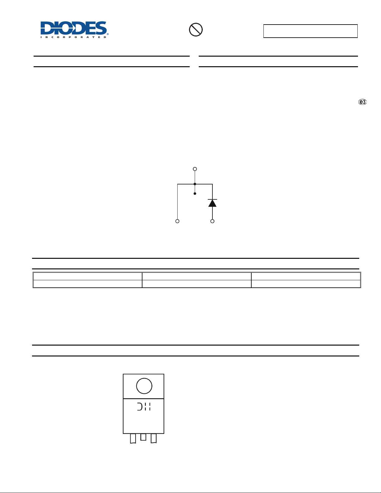
Polarity: See Diagram
Marking: Type Number
Weight: 2.24 grams (approximate)
Base
Cathode
1
13
Cathode
Package Pin Out
Confi
Anode
uration
MBR1635/ MBR1640
16A SCHOTTKY BARRIER RECTIFIER
Ordering Information (Note 3)
Part Number Case Packaging
MBR16xx* TO220AC 50/Tube
* xx = Device type, e.g. MBR1640
Notes: 1. EU Directive 2002/95/EC (RoHS) & 2011/65/EU (RoHS 2) compliant. All applicable RoHS exemptions applied.
2. See http://www.diodes.com/quality/lead_free.html for more information about Diodes Incorporated’s definitions of Halogen- and Antimony-free, "Green"
and Lead-free.
3. For packaging details, go to our website at http://www.diodes.com/products/packages.html.
Marking Information
MBR16xx
YYWW AB
MBR1635/ MBR1640
Document number: DS23011 Rev. 9 - 2
MBR16xx = Product Type Marking Code
B = Foundry and Assembly Code
YYWW = Date Code Marking
YY = Last two digits of year (ex: 10 = 2010)
WW = Week (01 - 53)
1 of 4
www.diodes.com
May 2013
© Diodes Incorporated
Page 2
R
GE F
O
R
R
C
URR
T
T
T
O
U
FORWARD CUR
R
T
Maximum Ratings (@T
Single phase, half wave, 60 Hz, resistive or inductive load.
For capacitive load, derate current by 20%.
= +25°C, unless otherwise specified.)
A
Characteristic Symbol
Peak Repetitive Reverse Voltage
Working Peak Reverse Voltage
DC Blocking Voltage
RMS Reverse Voltage
Average Rectified Output Current
(Note 4) @ TC = +125°C
Non-Repetitive Peak Forward Surge Current 8.3ms
Single Half Sine-Wave Superimposed on Rated Load
Thermal Characteristics
Characteristic Symbol Value Unit
Typical Thermal Resistance Junction to Case (Note 4)
Voltage Rate of Change (Rated VR)
Operating and Storage Temperature Range
MBR1635/ MBR1640
MBR
1635
V
V
RRM
RWM
35 40 V
VR
V
R(RMS)
I
IO
FSM
R
θJC
24.5 28 V
16 A
150 A
1.5
dV/dt 1000 V/µs
T
J, TSTG
-65 to +150
MBR
1640
Unit
C/W
C
Electrical Characteristics (@T
= +25°C, unless otherwise specified.)
A
Characteristic Symbol Value Unit
Forward Voltage Drop @ IF =16A, TC = +25°C
@ IF =16A, TC =+125°C
Peak Reverse Current @TC = +25°C
at Rated DC Blocking Voltage @ TC = +125°C
Typical Total Capacitance (Note 5)
Notes: 4. Thermal resistance junction to case mounted on heatsink.
5. Measured at 1.0MHz and applied reverse voltage of 4.0V DC.
20
VFM
IRM
CT
50
0.63
0.57
0.2
40
mA
450 pF
V
(A)
(A)
EN
16
EN
MBR1630 - MBR1645
10
D
12
WA
8
A
4
(AV)
I, AVE
0
050100150
T , CASE TEMPERATURE ( C)
C
°
Fig. 1 Forward Current Derating Curve
MBR1635/ MBR1640
Document number: DS23011 Rev. 9 - 2
2 of 4
www.diodes.com
S
1.0
ANE
AN
F
I, INS
0.1
0.2 0.4 0.6 0.8 1.0
V , INSTANTANEOUS FORWARD VOLTAGE (V)
F
Fig. 2 Typical Forward Voltage Characteristics
MBR1650 / MBR1660
May 2013
© Diodes Incorporated
Page 3

P
FORWAR
URGE CUR
RENT
C, CAPACITAN
C
TANT
O
US R
R
CUR
RENT
300
(A)
250
200
150
D S
100
EAK
50
FSM
I,
0
110100
100
(mA)
NUMBER OF CYCLES AT 60Hz
Fig. 3 Max Non-Repetitive Surge Current
4,000
E (pF)
1,000
T
100
0.1 1.0 10 100
V , REVERSE VOLTAGE (V)
Fig. 4 Typical Total Capacitance
MBR1635/ MBR1640
R
T= 25C
°
j
f = 1.0MHz
10
SE
1.0
EVE
ANE
0.1
R
0.01
I , INS
0 20 40 60 80 100 120 140
PERCENT OF RATED PEAK REVERSE VOLTAGE (%)
Fig. 5 Typical Reverse Characteristics
Package Outline Dimensions
Please see AP02002 at http://www.diodes.com/datasheets/ap02002.pdf for latest version.
Q
D
D1
b2
E
e1
P
H1
L1
L
b
MBR1635/ MBR1640
Document number: DS23011 Rev. 9 - 2
A
A1
SEATING PLANE
c
A2
3 of 4
www.diodes.com
TO220AC
Dim Min Typ Max
A 3.56 - 4.82
A1 0.51 - 1.39
A2 2.04 - 2.92
b 0.39 0.81 1.01
b2 1.15 1.24 1.77
c 0.356 - 0.61
D 14.22 - 16.51
D1 8.39 - 9.01
e1 5.08
E 9.66 - 10.66
H1 5.85 - 6.85
L 12.70 - 14.73
L1 - - 6.35
P 3.54 - 4.08
Q 2.54 - 3.42
All Dimensions in mm
May 2013
© Diodes Incorporated
Page 4

IMPORTANT NOTICE
DIODES INCORPORATED MAKES NO WARRANTY OF ANY KIND, EXPRESS OR IMPLIED, WITH REGARDS TO THIS DOCUMENT,
INCLUDING, BUT NOT LIMITED TO, THE IMPLIED WARRANTIES OF MERCHANTABILITY AND FITNESS FOR A PARTICULAR PURPOSE
(AND THEIR EQUIVALENTS UNDER THE LAWS OF ANY JURISDICTION).
Diodes Incorporated and its subsidiaries reserve the right to make modifications, enhancements, improvements, corrections or other changes
without further notice to this document and any product described herein. Diodes Incorporated does not assume any liability arising out of the
application or use of this document or any product described herein; neither does Diodes Incorporated convey any license under its patent or
trademark rights, nor the rights of others. Any Customer or user of this document or products described herein in such applications shall assume
all risks of such use and will agree to hold Diodes Incorporated and all the companies whose products are represented on Diodes Incorporated
website, harmless against all damages.
Diodes Incorporated does not warrant or accept any liability whatsoever in respect of any products purchased through unauthorized sales channel.
Should Customers purchase or use Diodes Incorporated products for any unintended or unauthorized application, Customers shall indemnify and
hold Diodes Incorporated and its representatives harmless against all claims, damages, expenses, and attorney fees arising out of, directly or
indirectly, any claim of personal injury or death associated with such unintended or unauthorized application.
Products described herein may be covered by one or more United States, international or foreign patents pending. Product names and markings
noted herein may also be covered by one or more United States, international or foreign trademarks.
This document is written in English but may be translated into multiple languages for reference. Only the English version of this document is the
final and determinative format released by Diodes Incorporated.
LIFE SUPPORT
Diodes Incorporated products are specifically not authorized for use as critical components in life support devices or systems without the express
written approval of the Chief Executive Officer of Diodes Incorporated. As used herein:
A. Life support devices or systems are devices or systems which:
1. are intended to implant into the body, or
2. support or sustain life and whose failure to perform when properly used in accordance with instructions for use provided in the
labeling can be reasonably expected to result in significant injury to the user.
B. A critical component is any component in a life support device or system whose failure to perform can be reasonably expected to cause the
failure of the life support device or to affect its safety or effectiveness.
Customers represent that they have all necessary expertise in the safety and regulatory ramifications of their life support devices or systems, and
acknowledge and agree that they are solely responsible for all legal, regulatory and safety-related requirements concerning their products and any
use of Diodes Incorporated products in such safety-critical, life support devices or systems, notwithstanding any devices- or systems-related
information or support that may be provided by Diodes Incorporated. Further, Customers must fully indemnify Diodes Incorporated and its
representatives against any damages arising out of the use of Diodes Incorporated products in such safety-critical, life support devices or systems.
Copyright © 2013, Diodes Incorporated
www.diodes.com
MBR1635/ MBR1640
MBR1635/ MBR1640
Document number: DS23011 Rev. 9 - 2
4 of 4
www.diodes.com
May 2013
© Diodes Incorporated
 Loading...