

Page 1
Features
• Voltage Controlled Small Signal Switch
• N-MOSFET with ESD Gate Protection
• Ideally Suited for Automated Assembly Processes
• Lead Free By Design/ROHS Compliant (Note 1)
• "Green" Device (Note 2)
Description
LMN400E01 is best suited for applications where the load needs to
be turned on and off using control circuits like micro-controllers,
comparators etc. particularly at a point of load. It features a discrete
pass transistor with stable V
voltage and can support continuous maximum current of 400 mA. It
also contains an ESD protected discrete N-MOSFET that can be used
as control. The component can be used as a part of a circuit or as a
stand alone discrete device.
which does not depend on input
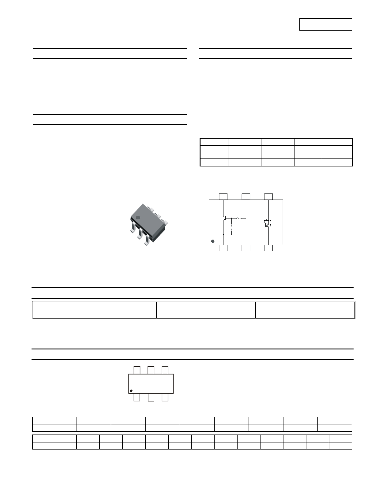
CE(SAT)
1
2
3
Top View
SOT363
6
5
4
LMN400E01
400mA LOAD SWITCH FEATURING PRE-BIASED
PNP TRANSISTOR AND ESD PROTECTED N-MOSFET
Mechanical Data
• Case: SOT363
• Case Material: Molded Plastic. "Green Molding" Compound. UL
Flammability Classification Rating 94V-0
• Moisture Sensitivity: Level 1 per J-STD-020C
• Terminal Connections: See Diagram
• Terminals: Finish - Matte Tin annealed over Alloy 42 leadframe.
Solderable per MIL- STD -202, Method 208
• Marking Information: See Page 8
• Ordering Information: See Page 8
• Weight: 0.006 grams (approximate)
•
Reference
Q1
Q2 N-MOSFET
Device Type R1(NOM) R2(NOM) Figure
PNP
Transistor
10K
220 2
⎯ ⎯
PNP
C_Q1
Q1
E_Q1
B_Q1
C
R2
B
220
E
R1
10K
1
2
G_Q2
S_Q2
456
S
Q2
G
NMOS
D
3
D_Q2
Top View
Internal Schematic
2
Ordering Information (Note 3)
Device Packaging Shipping
LMN400E01-7 SOT363 3000/Tape & Reel
Notes: 1. No purposefully added lead.
2. Diodes Inc.'s "Green" policy can be found on our website at http://www.diodes.com.
3. For packaging details, go to our website at http://www.diodes.com.
Marking Information
PM5
PM5 = Product Type Marking Code,
YM = Date Code Marking
YM
Y = Year, e.g., Y = 2011
M = Month, e.g., 9 = September
Date Code Key
Year 2006 2007 2008 2009 2010 2011 2012 2013
Code T U V W X Y Z A
Month Jan Feb Mar Apr May Jun Jul Aug Sep Oct Nov Dec
Code 1 2 3 4 5 6 7 8 9 O N D
LMN400E01
Document number: DS30750 Rev. 8 - 2
1 of 10
www.diodes.com
© Diodes Incorporated
July 2011
Page 2
Maximum Ratings, Total Device @T
= 25°C unless otherwise specified
A
Characteristic Symbol Value Unit
Power Dissipation (Note 4)
Power Derating Factor above 37.5°C
Output Current
Thermal Characteristics @T
= 25°C unless otherwise specified
A
Characteristic Symbol Value Unit
Operating and Storage Temperature Range
Thermal Resistance, Junction to Ambient Air (Note 4)
Maximum Ratings:
Pre-Biased PNP Transistor (Q1) @T
Characteristic Symbol Value Unit
Collector-Base Voltage
Collector-Emitter Voltage
Supply Voltage
Input Voltage
Output Current
= 25°C unless otherwise specified
A
V
V
CBO
CEO
Vcc
V
I
C
LMN400E01
PD
P
der
I
out
Tj, T
STG
R
JA
θ
in
-6 to +5 V
200 mW
1.6 mW/°C
400 mA
-55 to +150
625
°C
°C/W
-50 V
-50 V
-50 V
-400 mA
Maximum Ratings:
ESD Protected N-Channel MOSFET (Q2) @T
Characteristic Symbol Value Unit
Drain-Source Voltage
Drain Gate Voltage (RGS ≤ 1M Ohm) V
Gate-Source Voltage Continuous
Pulsed (tp<50 uS)
Drain Current (Note 4) Continuous (Vgs = 10V)
Pulsed (tp <10 uS, Duty Cycle <1%)
Continuous Source Current
Notes: 4. Device mounted on FR-4 PCB, 1 inch x 0.85 inch x 0.062 inch; pad layout as shown on Diodes Inc. suggested pad layout document AP02001,
which can be found on our website at http://www.diodes.com/datasheets/ap02001.pdf.
LMN400E01
Document number: DS30750 Rev. 8 - 2
= 25°C unless otherwise specified
A
V
DSS
DGR
V
GSS
I
D
I
S
2 of 10
www.diodes.com
60 V
60 V
+/-20
+/-40
300
800
V
mA
300 mA
© Diodes Incorporated
July 2011
Page 3
(BR)
(BR)
)
)
)
)
)
)
Electrical Characteristics: Pre-Biased PNP Transistor (Q1) @T
= 25°C unless otherwise specified
A
LMN400E01
Characteristic Symbol Min Typ Max Unit Test Condition
OFF CHARACTERISTICS (Note 5)
Collector-Base Cut Off Current
Collector-Emitter Cut Off Current
Collector-Base Breakdown Voltage
Collector-Emitter Breakdown Voltage
Input Off Voltage
Ouput Current
I
⎯ ⎯
CBO
I
⎯ ⎯
V
V
V
I
O(OFF)
CEO
CBO
CEO
I(OFF
-50
-50
-0.3 -0.55
⎯ ⎯
⎯ ⎯
⎯ ⎯
-500 nA
-1 uA
⎯
-1 uA
VCB = -50V, IE = 0
VCE = -50V, IB = 0
V
IC = -10uA, IE = 0
V
IC = -2mA, IB = 0
V
VCE = -5V, IC = -100uA
VCC = -50V, VI = 0V
ON CHARACTERISTICS (Note 5)
-0.15 V
-0.3 V
-0.5 V
-0.6 V
⎯ ⎯ V
⎯ ⎯ V
⎯
Collector-Emitter Saturation Voltage
DC Current Gain
Input On Voltage
Output Voltage (Equivalent to V
CE(SAT
Input Current
Base-Emitter Turn-on Voltage
Base-Emitter Saturation Voltage
V
) V
V
CE(SAT)
h
FE
V
I(ON
⎯
O(ON
I
⎯
I
V
BE(ON
BE(SAT
⎯ ⎯
⎯ ⎯
⎯ ⎯
⎯ ⎯
55 220
55 225
-3 -1.5
⎯
⎯
-0.1 -0.3 V
-18 -45 mA
-1.2 -1.6 V
-1.9 -2.5 V
Input Resistor (Base), +/- 30% R2 0.154 0.22 0.286
Pull-up Resistor (Base to Vcc supply), +/- 30% R1 7 10 13
Resistor Ratio (Input Resistor/Pullup resistor) R1/R2 36 45 55
V
KΩ
KΩ
⎯ ⎯
= -10mA, IB = -0.3mA
I
C
= -200mA, IB = -20mA
IC
IC = -400mA, IB= -40mA
IC = -500mA, IB = -50mA
= -5V, IC = -50mA
CE
= -5V, IC = -400mA
CE
VO = -0.3V, IC = -20mA
Io/II = -50mA /-2.5mA
VI = -5V
VCE = -5V, IC = -400mA
IC = -50mA, IB = -5mA
⎯
⎯
SMALL SIGNAL CHARACTERISTICS
= -10V, IE = -5mA,
V
Gain Bandwidth Product
Notes: 5. Short duration pulse test used to minimize self-heating effect.
LMN400E01
Document number: DS30750 Rev. 8 - 2
f
⎯
T
www.diodes.com
3 of 10
200
⎯
MHz
CE
f = 100MHz
July 2011
© Diodes Incorporated
Page 4

P, P
OWER
PAT
O
N
C
O
CTO
R
CUR
R
T
Electrical Characteristics:
ESD Protected N-Channel MOSFET (Q2) @T
Characteristic Symbol Min Typ Max Unit Test Condition
OFF CHARACTERISTICS (Note 5)
Drain-Source Breakdown Voltage
Zero Gate Voltage Drain Current
Gate-Body Leakage Current, Forward
Gate-Body Leakage Current, Reverse
ON CHARACTERISTICS (Note 5)
Gate Source Threshold Voltage
Static Drain-Source On-State Voltage
On-State Drain Current
Static Drain-Source On Resistance
Forward Transconductance
DYNAMIC CHARACTERISTICS
Input Capacitance
Output Capacitance
Reverse Transfer Capacitance
SWITCHING CHARACTERISTICS (Note 5)
Turn-On Delay Time
Turn-Off Delay Time
SOURCE-DRAIN (BODY) DIODE CHARACTERISTICS AND MAXIMUM RATINGS
Drain-Source Diode Forward On-Voltage
Maximum Continuous Drain-Source Diode Forward
Current (Reverse Drain Current)
Maximum Pulsed Drain-Source Diode Forward Current
Notes: 5. Short duration pulse test used to minimize self-heating effect.
250
200
(mW)
I
150
DISSI
100
D
50
Note 4
V
(BR)DSS
I
DSS
I
GSSF
I
GSSR
V
GS(th)
V
DS(on)
I
D(on)
R
DS(on)
g
C
C
C
td
td
V
I
I
SM
= 25°C unless otherwise specified
A
60
⎯ ⎯
⎯ ⎯
⎯ ⎯
1 1.6 2.5 V
⎯
⎯
500
⎯
⎯
80 260
FS
⎯ ⎯
iss
⎯ ⎯
oss
⎯ ⎯
rss
⎯ ⎯
(on)
⎯ ⎯
(off)
⎯
SD
⎯ ⎯
S
⎯ ⎯
⎯ ⎯
1
10
-10
0.09 1.9
0.6 3.75
⎯ ⎯
1.6 3
1.2 2
⎯
V
μA
μA
μA
V
mA
Ω
mS
50 pF
25 pF
5 pF
20 ns
40 ns
0.88 1.5 V
300 mA
800 mA
500
lb = 8mA
lb = 9mA
lb = 10mA
(mA)
EN
450
400
350
300
250
200
LLE
150
C
100
I,
V
= 0V, ID = 10uA
GS
= 0V, VDS = 60V
V
GS
VGS = 20V, VDS = 0V
= -20V, VDS = 0V
V
GS
VDS = VGS, ID = 0.25mA
= 5V, ID = 50mA
V
GS
VGS = 10V, ID = 500mA
V
= 10V,
GS
≥2*VDS(ON)
V
DS
V
= 5V, ID = 50mA
GS
= 10V, ID = 500mA
V
GS
VDS ≥2*V
V
V
I
D
R
DS(ON)
= -25V, VGS = 0V, f = 1MHz
DS
= 30V, VGS =10V,
DD
= 200mA,
= 25 Ohm, RL = 150 Ohm
G
VGS = 0V, IS = 300 mA*
lb = 7mA
lb = 6mA
lb = 5mA
LMN400E01
, ID = 200 mA
T = 25°C
A
lb = 4mA
lb = 3mA
lb = 2mA
lb = 1mA
50
0
0
50 75
25
T , AMBIENT TEMPERATURE (°C)
A
125 150 175
100
Fig. 3 Max Power Dissipation vs.
Ambient Temperatu r e
LMN400E01
Document number: DS30750 Rev. 8 - 2
4 of 10
www.diodes.com
0
00.51.0
1.5
2.0 2.5
V , COLLECTOR-BASE VOLTAGE (V)
CB
3.0
3.5
4.0
4.5
5.0
Fig. 4 Output Current vs.
Voltage Dr op (Pass Ele m ent PNP)
© Diodes Incorporated
5.5
July 2011
Page 5

C
O
CTO
R
OLT
C
CTOR
S
E E
MITTE
R
TAGE
A
S
E E
MITTE
R VOLT
A
E
C
CUR
R
N
T
G
N
AGE (V)
V
LLE
CE(SAT)
V,
(V)
Pre-Biased PNP Transistor Characteristics
I/I = 10
CB
T= 125C
°
A
T= 150C
°
A
I , COLLECTOR CURRENT (A)
C
Fig. 5 V vs. I @ I /I = 10
I/I = 10
CB
CE(SAT) C C B
T= -55C
A
T= 25C
A
T= 85C
°
A
I/I = 20
CB
LMN400E01
VOLTAGE (V)
°
°
OLLE
T = 150 C
CE(SAT)
V,
I , COLLECTOR CURRENT (A)
(V)
Fig. 6 V vs. I @ I /I = 20
I/I = 10
CB
V = 5V
CE
T= 125C
A
°
A
C
CE(SAT) C C B
°
T= 25C
A
T= 85C
°
A
T=-55C
°
A
°
G
VOL
T= -55C
°
A
T= 25C
A
T= 85C
°
A
T= -55C
°
T = 125 C
°
°
BE(ON)
V, B
I , COLLECTOR CURRENT (mA)
C
Fig. 8 V vs. I @ V = 5V
A
T = 150 C
°
A
BE(ON) C CE
A
T= 25C
°
A
T= 85C
°
A
BE(SAT)
V, BA
T= 125C
°
T= 150C
A
I , COLLECTOR CURRENT (mA)
C
Fig. 7 V vs. I @ I /I = 10
A
°
BE(SAT) C C B
V = 5V
CE
AI
E
FE
h, D
I , COLLECTOR CURRENT (mA)
C
Fig. 9 h vs. I @ V = 5V
LMN400E01
Document number: DS30750 Rev. 8 - 2
FE C CE
5 of 10
www.diodes.com
July 2011
© Diodes Incorporated
Page 6

R
CUR
RENT
R
N CUR
REN
T
R
C DRAIN
URC
LMN400E01
Typical N-Channel MOSFET (ESD Protected) Characteristics
T= 150C
°
T= 125C
A
T = 125C
°
A
A
°
V = 10V
GS
Pulsed
T = 85C
°
A
T= -55C
°
A
T= 25C
°
A
T= 85C
°
A
1.0
(A)
0.8
0.6
AIN
0.4
D
I, D
0.2
0
012 345
V , DRAIN-SOURCE VOLTAGE (V)
DS
Fig. 10 Output Characteristics
2
V= V
DS GS
V= 10V
DS
I = 1mA
D
1.5
Pulsed
V = 10V
DS
(A)
AI
D
I, D
V , GATE-SOURCE VOLTAGE
GS
Fig. 11 T ransfer Characteristics
10
E
T = 150C
Ω
-SO
°
A
1
T = -55C
°
, STATI
DS(on)
ON-RESISTANCE ( )
T = 25C
A
T = 0C
°
°
A
T = -25C
°
A
A
0.1
,
I DRAIN CURRENT(A)
Fig. 13 Static Drain-Source On-Resistance
D
vs. Drain Current
0.5
1
0
-25
-50
02550
T, JUNCTION TEMPERATURE (°C)
j
75 100
125 150
Fig. 12 Gate Threshold Voltage
vs. Junction Temperature
10
V = 5V
GS
Pulsed
T = 85C
T = 125 C
°
A
T = 150 C
°
A
Ω
T = 0C
T = 25C
°
ON-RESISTANCE ( )
DS(on)
R , STATIC DRAIN-SOURCE
A
°
A
T = -25C
°
A
Ω
T = -55C
°
A
°
A
ON-RESISTANCE ( )
DS(on)
R , STATIC DRAIN-SOURCE
0
1
I , DRAIN CURRENT (A)
D
Fig. 14 Static Drain-Source On-Resistance
vs. Dr ain Cu rr ent
LMN400E01
Document number: DS30750 Rev. 8 - 2
6 of 10
www.diodes.com
V GATE SOURCE VOLTAGE (V)
GS,
Fig. 15 Static Drain-Source On-Resistance
vs. G ate - S ource Voltage
© Diodes Incorporated
July 2011
Page 7

LMN400E01
V = 10V
GS
Pulsed
Ω
I = 300mA
D
I = 150mA
D
ON-RESISTANCE ( )
DS(on)
R , STATIC DRAIN-SOURCE
DR
I , REVERSE DRAIN CURRENT (A)
V = 0V
GS
Pulsed
T = 150 C
A
°
T= -55C
°
A
T = 125 C
A
T = 85C
A
T = 25C
°
A
T = 0C
°
A
T = -25C
A
°
°
°
0
T, JUNCTION TEMPERATURE ( C)
j
Static Drain-Source On-State Resistance
Fig. 16
vs. Junction Temperature
V = 10V
GS
°
T= -25C
T = 25°C
A
Pulsed
T= -55C
°
A
T= 125C
T = 150 C
A
V= 0V
S
I , REVERSE DRAIN CURRENT (A)
GS
FS
g , FORWARD TRANSCONDUCTANCE (mS)
A
°
°
A
T= 25C
°
A
°
T= 85C
°
A
1
LMN400E01
Document number: DS30750 Rev. 8 - 2
7 of 10
www.diodes.com
July 2011
© Diodes Incorporated
Page 8

LMN400E01
Application Details
PNP Transistor and ESD Protected N-MOSFET integrated as one in
LMN400E01 can be used as a discrete entity for general application
or as an integrated circuit to function as a Load Switch. When it is
used as the latter as shown in Fig. 20, various input voltage sources
can be used as long as it does not exceed the maximum ratings of
the device. These devices are designed to deliver continuous output
load current up to a maximum of 400 mA. The MOSFET Switch
draws no current, hence loading of control circuitry is prevented. Care
must be taken for higher levels of dissipation while designing for
higher load conditions. These devices provide high power and also
consume less space. The product mainly helps in optimizing power
usage, thereby conserving battery life in a controlled load system like
portable battery powered applications. (Please see Fig. 21 for one
example of a typical application circuit used in conjunction with a
voltage regulator as a part of power management system).
V
IN
Control
E
Q1 PNP
R1
10K
B
R2 220
D
C
Q2
S
N-MOSFET
G
Fig. 20 Circuit Diagram
V
OUT
LOAD
U1
Vin
Control Logic
Circuit (PIC,
Comparator
etc)
GND
LMN400E01
Document number: DS30750 Rev. 8 - 2
OUT1
5V Supply
Load Switch
U2
1
Vin
Control
2
3
E_Q1
G_Q2
D_Q2
LMN400E01
Diodes Inc.
Fig. 21 Typical Application Circuirt
www.diodes.com
C_Q1
B_Q1
S_Q2
8 of 10
U3
Point of
Vout
6
5
GND
4
IN OUT
Voltage Regulator
Load
July 2011
© Diodes Incorporated
Page 9

Package Outline Dimensions
K
J
A
SOT-363
Dim Min Max
A 0.10 0.30
B C
B 1.15 1.35
C 2.00 2.20
D 0.65 Nominal
F 0.30 0.40
H
H 1.80 2.20
J - 0.10
M
K 0.90 1.00
L 0.25 0.40
D
L
F
M 0.10 0.25
α
0°
8°
All Dimensions in mm
Suggested Pad Layout
G
Z
EE
Dimensions Value (mm)
Z 2.5
G 1.3
X 0.42
C
Y 0.6
C 1.9
E 0.65
Y
X
LMN400E01
Document number: DS30750 Rev. 8 - 2
9 of 10
www.diodes.com
LMN400E01
July 2011
© Diodes Incorporated
Page 10

IMPORTANT NOTICE
DIODES INCORPORATED MAKES NO WARRANTY OF ANY KIND, EXPRESS OR IMPLIED, WITH REGARDS TO THIS DOCUMENT,
INCLUDING, BUT NOT LIMITED TO, THE IMPLIED WARRANTIES OF MERCHANTABILITY AND FITNESS FOR A PARTICULAR PURPOSE
(AND THEIR EQUIVALENTS UNDER THE LAWS OF ANY JURISDICTION).
Diodes Incorporated and its subsidiaries reserve the right to make modifications, enhancements, improvements, corrections or other changes
without further notice to this document and any product described herein. Diodes Incorporated does not assume any liability arising out of the
application or use of this document or any product described herein; neither does Diodes Incorporated convey any license under its patent or
trademark rights, nor the rights of others. Any Customer or user of this document or products described herein in such applications shall assume
all risks of such use and will agree to hold Diodes Incorporated and all the companies whose products are represented on Diodes Incorporated
website, harmless against all damages.
Diodes Incorporated does not warrant or accept any liability whatsoever in respect of any products purchased through unauthorized sales channel.
Should Customers purchase or use Diodes Incorporated products for any unintended or unauthorize d application, Customers shall indemnify and
hold Diodes Incorporated and its representatives harmless against all claims, damages, expenses, and attorney fees arising out of, directly or
indirectly, any claim of personal injury or death associated with such unintended or unauthorized application.
Products described herein may be covered by one or more United States, international or foreign patents pending. Product names and markings
noted herein may also be covered by one or more United States, international or foreign trademarks.
LIFE SUPPORT
Diodes Incorporated products are specifically not authorized for use as critical components in life support devices or systems without the express
written approval of the Chief Executive Officer of Diodes Incorporated. As used herein:
A. Life support devices or systems are devices or systems which:
1. are intended to implant into the body, or
2. support or sustain life and whose failure to perform when properly used in accordance with instructions for use provided in the
labeling can be reasonably expected to result in significant injury to the user.
B. A critical component is any component in a life support device or system whose failure to perform can be reasonably expected to cause the
failure of the life support device or to affect its safety or effectiveness.
Customers represent that they have all necessary expertise in the safety and regulatory ramifications of their life support devices or systems, and
acknowledge and agree that they are solely responsible for all legal, regulatory and safety-related requirements concerning their products and any
use of Diodes Incorporated products in such safety-critical, life support devices or systems, notwithstanding any devices- or systems-related
information or support that may be provided by Diodes Incorporated. Further, Customers must fully indemnify Diodes Incorporated and its
representatives against any damages arising out of the use of Diodes Incorporated products in such safety-critical, life support devices or systems.
Copyright © 2011, Diodes Incorporated
www.diodes.com
LMN400E01
LMN400E01
Document number: DS30750 Rev. 8 - 2
10 of 10
www.diodes.com
July 2011
© Diodes Incorporated
 Loading...