

Page 1
Lead-free Green
200 mA LOAD SWITCH FEATURING PRE-BIASED PNP TRANSISTOR AND N-MO SFET
S
D
G
C
E
B
Q2
NMOS
R3
37K
R2
470
Q1
PNP
R1
10K
1
2
3
4
56
C_Q1
E_Q1
G_Q2
D_Q2
S_Q2
B_Q1
DSNM6047_DIE
DDTB142JU_DIE
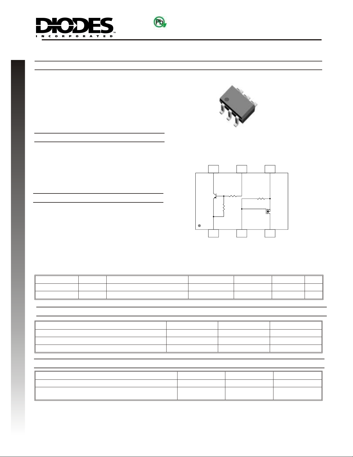
Fig. 2 Schematic and Pin Configuration
1
2
3
4
5
6
TCUDORP WEN
General Description
• LMN200B01 is best suited for applications where the load
needs to be turned on and off using control circuits like
micro-controllers, comparators, etc., particularly at a point
of load. It features a discrete pass transistor with stable
V
which does not depend on the input voltage and
CE(SAT)
can support continuous maximum current of 200 mA. It
also contains a discrete N-MOSFET that can be used as
control. This N-MOSFET also has a built-in pull down
resistor at its gate. The component can be used as a part
of a circuit or as a stand alone discrete device.
LMN200B01
WITH PULL DOWN RESISTOR
Features
Fig. 1: SOT-26
• Voltage Controlled Small Signal Switch
• N-MOSFET with Gate Pull-Down Resistor
• Surface Mount Package
• Ideally Suited for Automated Assembly Processes
• Lead Free By Design/ROHS Compliant (Note 1)
• "Green" Device (Note 2)
Mechanical Data
• Case: SOT-26
• Case Material: Molded Plastic, “Green” Molding
Compound. UL Flammability Classification Rating 94V-0
• Moisture sensitivity: Level 1 per J-STD-020C
• Terminal Connections: See Diagram
• Terminals: Finish - Matte Tin annealed over Copper
leadframe. Solderable per MIL-STD-202, Method 208
• Marking & Type Code Information: See Last Page
• Ordering Information: See Last Page
• Weight: 0.016 grams (approximate)
Sub-Components Reference Device Type R1 (NOM) R2 (NOM) R3 (NOM) Figure
DDTB142JU_DIE
DSNM6047_DIE
Q1 PNP Transistor 10K 470 2
Q2 N-MOSFET 37K 2
Maximum Ratings, Total Device
Characteristic Symbol Value Unit
Power Dissipation (Note 3)
Power Derating Factor above 125°C
Output Current
Thermal Characteristics
Characteristic Symbol Value Unit
Junction Operation and Storage Temperature Range
Thermal Resistance, Junction to Ambient Air (Note3)
(Equivalent to one heated junction of PNP transistor)
Notes: 1. No purposefully added lead.
2. Diodes Inc.'s "Green" policy can be found on our website at http://www.diodes.com/products/lead_free/index.php.
3. Device mounted on FR-4 PCB, 1 inch x 0.85 inch x 0.062 inch; pad layout as shown on Diodes Inc. suggested pad layout
document AP02001, which can be found on our website at http://www.diodes.com/datasheets/ap02001.pdf.
DS30651 Rev. 7 - 2 1 of 10 LMN200B01
@ TA = 25°C unless otherwise specified
P
d
P
der
I
out
Tj,T
stg
R
θJA
300
2.4 mW/°C
200 mA
-55 to +150 °C
417 °C/W
www.diodes.com Diodes Incorporated
mW
Page 2
TCUDORP WEN
Maximum Ratings:
Sub-Component Device: Pre-Biased PNP Transistor (Q1)
Characteristic Symbol Value Unit
Collector-Base Voltage
Collector-Emitter Voltage
Supply Voltage
Input Voltage
Output Current
Sub-Component Device:
N-MOSFET with Gate Pull-Down Resistor (Q2)
Characteristic Symbol Value Unit
Drain-Source Voltage
Drain Gate Voltage (RGS ≤1MΩ) V
Gate-Source Voltage Continuous
Pulsed (tp<50 uS) +/-40
Drain Current (Page 1: Note 3) Continuous (Vgs = 10V)
Pulsed (tp <10 uS, Duty Cycle <1%) 800
Continuous Source Current
V
CBO
V
CEO
V
cc
V
in
I
C
@ TA = 25°C unless otherwise specified
V
DSS
DGR
V
GSS
I
D
I
S
@ TA = 25°C unless otherwise specified
-50 V
-50 V
-50 V
+5 to -6 V
-200 mA
60 V
60 V
+/-20
115
115 mA
V
mA
DS30651 Rev. 7 - 2 2 of 10 LMN200B01
www.diodes.com
Page 3
TCUDORP WEN
Electrical Characteristics: Pre-Biased PNP Transistor (Q1)
@ TA = 25°C unless otherwise specified
Characteristic Symbol Min Typ Max Unit Test Condition
OFF CHARACTERISTICS
Collector-Base Cut Off Current
Collector-Emitter Cut Off Current
Emitter-Base Cut Off Current
Emitter-Base Cut Off Current
Collector-Base Breakdown Voltage
Collector-Emitter Breakdown Voltage
Output Voltage
Output Current (leakage current same as I
) I
CEO
I
CBO
I
CEO
I
EBO
V
(BR)CBO
V
(BR)CEO
V
I(OFF)
V
O(OFF)
-100 nA
-500 nA
-0.5 -1 mA
-50 V
-50 V
-0.55 -0.3 V
-4.9 V
OH
-500 nA
VCB = -50V, IE = 0
V
V
IC = -10µA, IE = 0
IC = -2 mA, IB = 0
VCE = -5V, IC = -100µA
VCC = -5V, VB = -0.05V, RL = 1K
VCC = -50V, VI = 0V
ON CHARACTERISTICS
IC = -10 mA, IB = -0.5 mA
IC = -50mA, IB = -5mA
IC = -20mA, IB = -1mA
IC = -100mA, IB= -10mA
IC = -200mA, IB= -10mA
IC = -200mA, IB = -20mA
IC = -200mA, IB = -10mA
VCE = -5V, IC = -20 mA
VCE = -5V, IC = -50 mA
VCE = -5V, IC = -100 mA
VCE = -5V, IC = -200 mA
VO = -0.3V, IC = -2 mA
VCC = -5V, VB = -2.5V,
Io/I
VI = -5V
VCE = -5V, IC = -200mA
IC = -50mA, IB = -5mA
V
IC = -80mA, IB = -8mA
Collector-Emitter Saturation Voltage
Equivalent on-resistance*
DC Current Gain
Input On Voltage
Output Voltage (equivalent to V
CE(SAT)
Input Current
Base-Emitter Turn-on Voltage
Base-Emitter Saturation Voltage
or V
) V
O(on)
V
CE(SAT)
R
CE(SAT)
h
V
I(ON)
V
BE(ON)
V
BE(SAT)
-0.15 V
-0.2 V
-0.2 V
-0.25 V
-0.25 V
-0.3 V
1.5 Ω
60 150
FE
60 215
60 245
60 250
-2.45 -0.7 V
OL
I
-0.065 -0.15 V
-9.2 -13 mA
i
-1.125 -1.3 V
-3.2 -3.6
-4.55 -5.5
Input Resistor (Base), +/- 30% R2 0.47 KΩ
Pull-up Resistor (Base to Vcc supply), +/- 30% R1 10 KΩ
Resistor Ratio (Input Resistor/Pullup resistor), +/ -20% R1/R2 21
SMALL SIGNAL CHARACTERISTICS
Transition Frequency (gain bandwidth product)
Collector capacitance, (Ccbo-Output Capacitance)
f
T
C
200 MHz
20 pF
C
VCE = -10V, IE = -5mA,
f = 100MHz
VCB = -10V, IE = 0A,
f = 1MHz
= -50V, IB = 0
CE
= -5V, IC = 0
EB
-50mA /-2.5mA
I =
* Pulse Test: Pulse width, tp<300 µS, Duty Cycle, d<=0.02.
DS30651 Rev. 7 - 2 3 of 10 LMN200B01
www.diodes.com
Page 4

TCUDORP WEN
0
50
25 50
75
100 125
150
175
P , POWER DISSIPATION (mW)
D
T , AMBIENT TEMPERA TURE (°C)
A
Fig. 3, Max Power Dissipation vs Ambient Temperature
100
150
300
350
200
250
0
Electrical Characteristics:
N-MOSFET with Gate Pull-Down Resistor (Q2)
Characteristic Symbol Min Typ Max Unit Test Condition
OFF CHARACTERISTICS (Note 4)
Drain-Source Breakdown Voltage, BVDSS
Zero Gate Voltage Drain Current (Drain Leakage
Current)
Gate-Body Leakage Current, Forward
Gate-Body Leakage Current, Reverse
V
(BR)DSS
I
DSS
I
GSSF
I
GSSR
ON CHARACTERISTICS (Note 4)
Gate Source Threshold Voltage (Control Supply
Voltage)
Static Drain-Source On-State Voltage
On-State Drain Current
Static Drain-Source On Resistance
Forward Transconductance
V
V
DS(on)
I
R
GS(th)
D(on)
DS(on)
g
FS
Gate Pull-Down Resistor, +/- 30% R3 37 KΩ
DYNAMIC CHARACTERISTICS
Input Capacitance
Output Capacitance
Reverse Transfer Capacitance
C
iss
C
oss
C
rss
SWITCHING CHARACTERISTICS*
Turn-On Delay Time
Turn-Off Delay Time
td
(on)
td
(off)
SOURCE-DRAIN (BODY) DIODE CHARACTERISTICS AND MAXIMUM RATINGS
Drain-Source Diode Forward On-Voltage
Maximum Continuous Drain-Source Diode Forward
Current (Reverse Drain Current)
Maximum Pulsed Drain-Source Diode Forward
Current
* Pulse Test: Pulse width, tp<300 µS, Duty Cycle, d<=0.02.
Notes: 4. Short duration test pulse used to minimize self-heating effect.
V
SD
I
S
I
SM
Typical Characteristics
@ TA = 25°C unless otherwise specified
60 V
1 µA
0.95 mA
-0.95 mA
1 1.86 2.2 V
0.08 1.5
0.15 3.75
500 mA
1.55 3
1.4 2
80 240
80 350
V
V
V
V
VDS = VGS, ID = 0.25mA
VGS = 5V, ID = 50mA
V
VGS = 10V, ID = 115mA
VGS = 10V,
VDS ≥2 V
VGS = 5V, ID = 50mA
Ω
VGS = 10V, ID = 500mA
VDS ≥2 V
mS
VDS ≥2 V
50 pF
25 pF
VDS = -25V, VGS = 0V,
ƒ= 1MHz
5 pF
20 ns
40 ns
0.88 1.5 V
VDD = 30V, VGS =10V,
ID = 200mA,
RG = 25Ω, RL = 150Ω
VGS = 0V, IS = 115 mA*
115 mA
800 mA
= 0V, ID = 10µA
GS
=0V, VDS = 60V
GS
= 20V, VDS = 0V
GS
= -20V, VDS = 0V
GS
DS(ON)
DS(ON)
DS(ON)
, ID = 115 mA
, ID = 200 mA
DS30651 Rev. 7 - 2 4 of 10 LMN200B01
www.diodes.com
Page 5

TCUDORP WEN
Typical Pre-Biased PNP Transistor (Q1) Characteristics
I , COLLECTOR CURRENT (A)
C
Fig. 5 V vs. I
CE(SAT) C
V , COLLECTOR VOLTAGE (V)
CE(SAT)
0.6
0
0.1
0.2
0.3
0.4
0.5
0.01
0.1
1
I /I = 20
CB
T=
A
150°C
T=
A
125°C
T=
A
25°C
T=
A
85°C
T=
A
-55°C
I , COLLECTOR CURRENT (A)
C
Fig. 4 V vs. I
CE(SAT) C
V , COLLECTOR VOLTAGE (V)
CE(SAT)
0.01
0.1
1
0
0.1
0.2
0.3
0.4
I /I = 10
CB
T= A 150°C
T=
A
125°C
T=
A
-55°C
T=
A
85°C
T=
A
25°C
I , COLLECTOR CURRENT (mA)
C
Fig. 7 V vs. I
BE(ON) C
V , BASE EMITTER VOLTAGE (V)
BE(ON)
1
10
100
1000
0
0.5
1
1.5
2
2.5
3
I /I = 10
CB
V = 5V
CE
T=
A
85°C
T=
A
125°C
T=
A
150°C
T=
A
25°C
T=
A
-55°C
I , COLLECTOR CURRENT (mA)
C
Fig. 6 V vs. I
BE(SAT) C
V , BASE EMITTER VOLTAGE (V)
BE(SAT)
1
10 100 1000
0
5
10
15
20
25
30
I /I = 10
CB
T=
A
150°C
T=
A
125°C
T=
A
25°C
T=
A
-55°C
T=
A
85°C
I , COLLECTOR CURRENT (mA)
C
Fig. 8 h vs. I
FE C
h , DC CURRENT GAIN
FE
1
10
100
1000
0
100
200
300
400
T=
A
125°C
V = 5V
CE
T=
A
25°C
T= A -55°C
T=
A
150°C
T=
A
85°C
DS30651 Rev. 7 - 2 5 of 10 LMN200B01
www.diodes.com
Page 6

V , GATE-SOURCE VOLTAGE (V)
GS
Fig. 10 Transfer Characteristics
I , DRAIN CURRENT (A)
D
0
0.2
0.4
0.6
0.8
1
1.2
1.4
0
1
2
3
4
5
T=
A
-55°C
T= A 25°C
T=
A
85°C
T=
A
125°C
T=
A
150°C
V = 10V
DS
T , JUNCTION TEMPERATURE (°C)
J
Fig. 11 Gate Threshold Voltage
vs. Junction Temperature
0
1.2
1.4
1.6
1.8
2
2.2
-50
-75
-25
0
25
50
75
100
125
150
V GATE THRESHOLD VOLTAGE (V)
GS(th),
V = 10V
DS
V= V
DS GS
I = 0.25mA
D
Pulsed
I , DRAIN CURRENT (A)
D
Fig. 12 Static Drain-Source On-Resistance
vs. Drain Current
0.001
0.01
0.1
1
0
1
2
3
4
5
V = 5V
GS
Pulsed
T = -55°C
A
T = 25°C
A
T = 125°C
A
T = 150°C
A
T = 85°C
A
1
I , DRAIN CURRENT (A)
D
Fig. 13 Static Drain-Source On-Resistance
vs. Drain Current
4
0
1
2
3
0.001
0.01
0.1
V = 10V
GS
Pulsed
T = 150°C
A
T = 125°C
A
T = 85°C
A
T = 25°C
A
T = -55°C
A
0
V GATE SOURCE VOLTAGE (V)
GS,
Fig. 14 Static Drain-Source On-Resistance
vs. Gate-Source Voltage
1
2
3
4
5
6
7
0
2
4
6
8
10
12 14
16 18
20
I = 115mA
D
I = 50mA
D
T = 25°C
A
Pulsed
V , DRAIN-SOURCE VOLTAGE (V)
DS
Fig. 9 Output Characteristics
I , DRAIN CURRENT (A)
D
T = 25°C
A
0
1
2
3
4
5
6
7
0
0.2
0.4
0.6
0.8
1.0
1.2
1.4
1.6
1.8
V = 8V
GS
V = 10V
GS
V = 3V
GS
V = 4V
GS
V = 5V
GS
V = 6V
GS
TCUDORP WEN
Typical N-Channel MOSFET (Q2) Characteristics
DS30651 Rev. 7 - 2 6 of 10 LMN200B01
www.diodes.com
Page 7

T, JUNCTION TEMPERATURE (°C)
j
Fig. 15 Static Drain-Source On-State Resistance
vs. Junction Temperature
0.5
1
1.5
2
2.5
-75
-50 -25
0 25
50
75
100 125
150
V = 10V
GS
Pulsed
I = 115mA
D
I = 50mA
D
I , REVERSE DRAIN CURRENT (A)
S
0.001
0.01
0.1
1
0
0.5
1
1.5
V , SOURCE-DRAIN VOLTAGE (V)
SD
Fig. 16 Reverse Drain Current
vs. Source-Drain Voltage
V = 5V
GS
Pulsed
T = 150°C
A
T = 125°C
A
T = 85°C
A
T = 25°C
A
T = -55°C
A
0.5
1
1.5
2
2.5
0.001
0.01
0.1
1
0
I , REVERSE DRAIN CURRENT (A)
S
V , BODY DIODE FORWARD VOLTAGE (V)
SD
Fig. 17 Reverse Drain Current
vs. Body Diode Forward Voltage
=25 C
T = 25°C
A
Pulsed
V = 5V
GS
V = 10V
GS
g , FORWARD TRANSCONDUCTANCE (mS)
FS
I , DRAIN CURRENT (A)
D
Fig. 18 Forward Transconductance
vs. Drain Current (V > I R )
DS D DS(ON)
0
100
200
300
400
500
600
700
800
900
0
0.2
0.4
0.6
0.8
T=
A
-55°C
T=
A
25°C
T=
A
85°C
T=
A
150°C
T=
A
125°C
TCUDORP WEN
www.diodes.com Diodes Incorporated
DS30651 Rev. 7 - 2 7 of 10 LMN200B01
Page 8

TCUDORP WEN
Vin
Control
D
E
S
B
G
C
Q1 PNP
Q2 NMOS
R2 470
R1
10K
R3
37K
LOAD
DDTB142JU
DSNM6047
Vout
5v Supply
Vout
Gnd
Vin
Control
U2
Voltage Regulator
IN OUT
Control Logic
Circuit (PIC,
Comparator
etc)
U1
Vin
OUT1
GND
Diodes Inc.
U3
LNM200B01
1
3
2
4
5
6
E_Q1
D_Q2
G_Q2
S_Q2
B_Q1
C_Q1
Load Switch
Point of
Load
Application Details
• PNP Transistor (DDTB142JU) and N-MOSFET
(DSNM6047) with gate pull-down resistor integrated
as one in LMN200B01 can be used as a discrete
entity for general purpose applications or as an
integrated circuit to function as a Load Switch. When
it is used as the latter as shown in Fig 19, various
input voltage sources can be used as long as it does
not exceed the maximum ratings of the device.
These devices are designed to deliver continuous
output load current up to a maximum of 200 mA. The
MOSFET Switch draws no current, hence loading of
control circuit is prevented. Care must be taken for
higher levels of dissipation while designing for higher
load conditions. These devices provide high power
and also consume less space. The product mainly
helps in optimizing power usage, thereby conserving
battery life in a controlled load system like portable
battery powered applications. (Please see Fig. 20
for one example of a typical application circuit used
in conjunction with voltage regulator as a part of a
power management system)
Fig. 19 Circuit Diagram
Typical Application Circuit
DS30651 Rev. 7 - 2 8 of 10 LMN200B01
Fig. 20
www.diodes.com
Page 9

TCUDORP WEN
PM1
YM
Ordering Information
(Note 5)
Device
LMN200B01-7
Note: 5. For Packaging Details, go to our website at http://www.diodes.com/datasheets/ap02007.pdf.
Marking Code Packaging Shipping
PM1 SOT-26 3000/Tape & Reel
Marking Information
PM1 = Product Type Marking Code,
YM = Date Code Marking
Y = Year ex: T = 2006
M = Month ex: 9 = September
Fig. 21
Date Code Key
Year 2006
Code
Month Jan Feb March Apr May Jun Jul
Code
1 2 3 4 5 6 7
T
2007 2008 2009
U V W
Aug Sep Oct Nov Dec
8 9 O N D
DS30651 Rev. 7 - 2 9 of 10 LMN200B01
www.diodes.com
Page 10

A
M
J
L
D
F
B
C
H
K
IMPORTANT NOTICE
Diodes, Inc. and its subsidiaries reserve the right to make changes without further notice to any product herein to make corrections, modifications, enhance-
ments, improvements, or other changes. Diodes, Inc. does not assume any liability arising out of the application or use of any product described herein;
neither does it convey any license under its patent rights, nor the rights of others. The user of products in such applications shall assume all risks of such
use and will agree to hold Diodes Incorporated and all the companies whose products are represented on our website, harmless against all damages.
LIFE SUPPORT
The products located on our website at www.diodes.com are not recommended for use in life support systems where a failure or malfunction of the
component may directly threaten life or cause injury without the expressed written approval of Diodes Incorporated.
X
Z
Y
C
E
E
G
TCUDORP WEN
Mechanical Details
Fig. 22
Suggested Pad Layout: (Based on IPC-SM-782)
SOT-26
Dim Min Max
A
B
C
D
F
H
J
K
L
M
α
0.35 0.5 0.38
1.5 1.7 1.6
2.7 3 2.8
- - 0.95
- - 0.55
2.9 3.1 3
0.013 0.1 0.05
1 1.3 1.1
0.35 0.55 0.4
0.1 0.2 0.15
0° 8° -
All Dimensions in mm
Typ
Figure 23
Dimensions
Z
G
X
Y
C
E
Fig. 23
SOT-26*
3.2
1.6
0.55
0.8
2.4
0.95
DS30651 Rev. 7 - 2 10 of 10 LMN200B01
www.diodes.com
 Loading...