

Page 1
Please click here to visit our online spice models database.
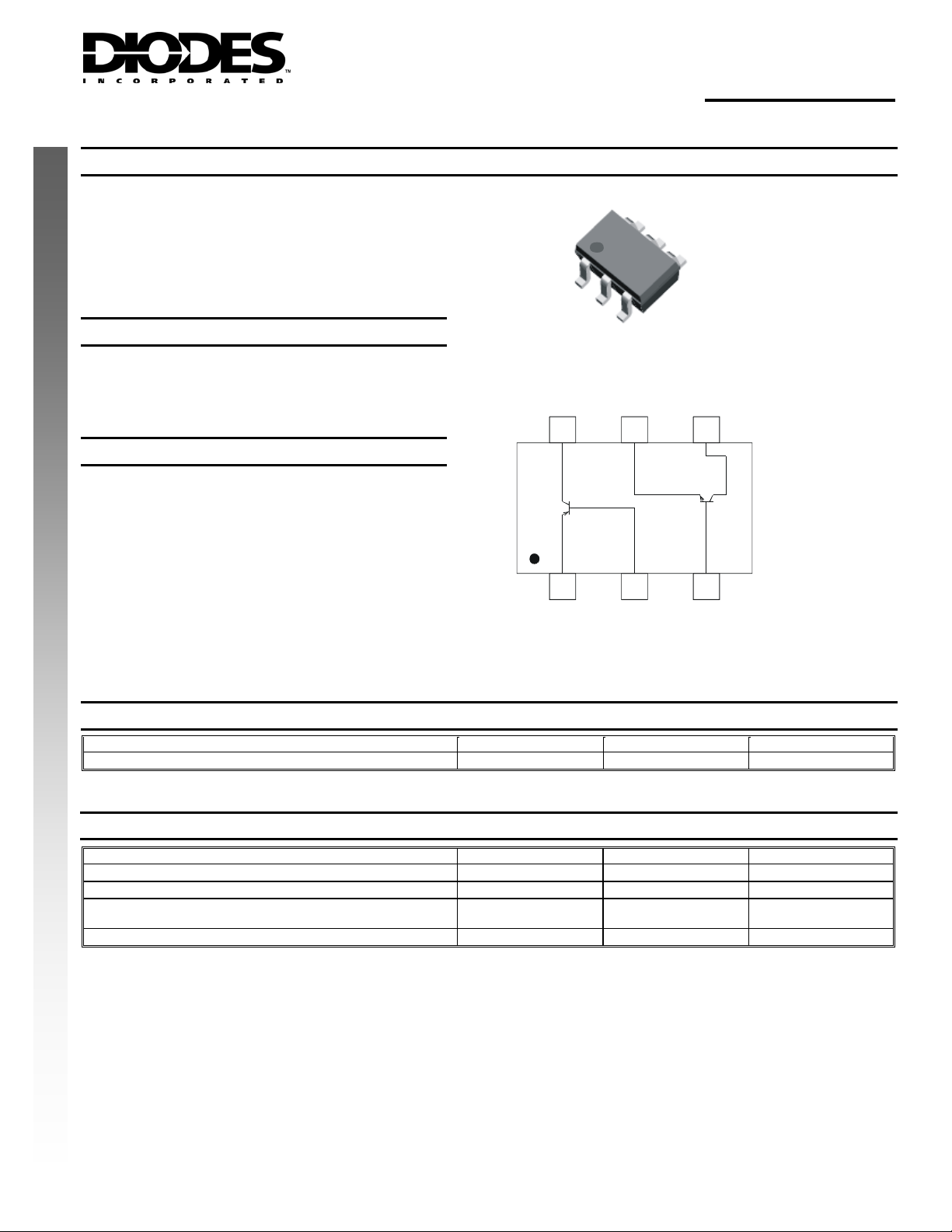
150 mA LOAD SWITCH FEATURING COMPLEMENTARY BIPOLAR TRANSISTORS
General Description
• LMN150B01 is best suited for applications where the load
needs to be turned on and off using control circuits like
micro-controllers, comparators etc. particularly at a point of
load. It features a discrete PNP pass transistor with stable
V
which does not depend on the input voltage and can
ce_sat
support maximum continuous current of 150 mA up to
125 °C (see fig. 1). It also contains a discrete NPN that can
be used as a control. The component devices can be used
as a part of a circuit or as standalone discrete devices.
Features
• Epitaxial Planar Die Construction
• Ideally
• Lead Free By
• "Green" Dev
NEW PRODUCT
Suited for Automated Assembly Processes
Design/ROHS Compliant (Note 1)
ice (Note 2)
Mechanical Data
• Case: SOT-26
• Case Material: Molded Plastic. "Green Molding"
Compound. UL Flammability
• Moisture Sensitivity
• Terminal Connections: See Diagram
• Terminals: Finish - Matte Tin annealed over Copper
leadframe. Solderable per MIL- STD -202, Method 208
• Marking Information: See Page 6
• Ordering Information: See Page 6
• Weight: 0.016 grams (approximate)
: Level 1 per J-STD-020C
Classification Rating 94V-0
LBN150B01
6
5
4
1
2
3
SOT-26
EQ2CQ1
6
Q1
1
EQ1
Schematic and Pin Configuration
5
23
BQ1
CQ2
4
Q2
BQ2
Maximum Ratings, Total Device @T
Characteristic Symbol Value Unit
Output Current
Thermal Characteristics @T
Characteristic Symbol Value Unit
Power Dissipation (Note 3)
Thermal Resistance, Junction to Ambient Air (Note 3)
(Equivalent to one heated junction of PNP transistor)
Junction Operation and Storage Temperature Range
Notes: 1. No purposefully added lead.
DS30749 Rev. 4 - 2 1 of 7
2 . Diodes Inc.'s "Green" policy can be found on our website at http://www.diodes.com/products/lead_free/index.php.
3. Device mounted on FR-4 PCB, 1 inch x 0.85 inch x 0.062 inch; pad layout as shown on Page 7.
= 25°C unless otherwise specified
A
= 25°C unless otherwise specified
A
I
out
P
D
P
der
R
JA
θ
TJ, T
STG
www.diodes.com
150 mA
300 mW
2.33
417
-55 to +150
mW/°C Power Derating Factor above 120 °C
°C/W
°C
LBN150B01
© Diodes Incorporated
Page 2
Maximum Ratings: Discrete PNP Transistor (Q1) @T
A
Characteristic Symbol Value Unit
Collector-Base Voltage
Collector-Emitter Voltage
Emitter-Base Voltage
Output Current - continuous (Note 4)
V
CBO
V
CEO
V
EBO
I
C
Maximum Ratings: Discrete NPN Transistor (Q2) @T
Characteristic Symbol Value Unit
Collector-Base Voltage
Collector-Emitter Voltage
Emitter-Base Voltage
Output Current - continuous (Note 4)
V
CBO
V
CEO
V
EBO
I
C
Electrical Characteristics: Discrete PNP Transistor (Q1) @T
NEW PRODUCT
OFF CHARACTERISTICS (Note 4)
Collector-Base Breakdown Voltage
Collector-Emitter Breakdown Voltage
Emitter-Base Breakdown Voltage
Collector Cutoff Current
Base Cutoff Current
Collector-Base Cut Off Current
Collector-Emitter Cut Off Current
Emitter-Base Cut Off Current
ON CHARACTERISTICS (Note 4)
DC Current Gain
Collector-Emitter Saturation Voltage
Equivalent on-resistance
Base-Emitter Turn-on Voltage
Base-Emitter Saturation Voltage
SMALL SIGNAL CHARACTERISTICS
Output Capacitance
Input Capacitance
Input Impedance
Voltage Feedback ratio
Small Signal Current Gain
Output Admittance
Current Gain-Bandwidth Product
Noise Figure NF
SWITCHING CHARACTERISTICS
Delay Time
Rise Time
Storage Time
Fall Time
Notes: 4. Short duration pulse test used to minimize self-heating effect.
Characteristic Symbol Min Max Unit Test Condition
V
V
V
I
CEX
I
I
CBO
I
CEO
I
EBO
h
V
CE(SAT)
R
CE(SAT)
V
BE(ON)
V
BE(SAT)
C
C
h
h
h
h
CBO
CEO
EBO
BL
FE
OBO
IBO
IE
RE
FE
OE
f
T
t
d
t
r
t
s
t
f
-40
-40
-6
⎯
⎯
⎯
⎯
⎯
105
110
120
90
32
10
⎯
⎯
⎯
⎯
⎯
⎯
⎯
⎯
⎯
2 12
0.1 10 x 10E-4
100 400
3 60
250
⎯
⎯
⎯
⎯
⎯
⎯
⎯
⎯
-50 nA
-50 nA
-50 nA
-50 nA
-50 nA
⎯ ⎯
⎯ ⎯
⎯ ⎯
⎯ ⎯
⎯ ⎯
⎯ ⎯
-0.08
-0.15
-0.5
2.5
-0.92 V
-0.95
-1.1
4 pF
8 pF
⎯
4 dB
35 ns
35 ns
225 ns
75 ns
= 25°C unless otherwise specified
-40 V
-40 V
-6 V
-200 mA
= 25°C unless otherwise specified
A
60 V
40 V
6 V
200 mA
= 25°C unless otherwise specified
A
V
V
V
V
Ω
V
= -10uA, IE = 0
I
C
= -1.0mA, IB = 0
I
C
= -10μA, IC = 0
I
E
= -30V, V
V
CE
= -30V, V
V
CE
= -30V, IE = 0
V
CB
= -30V, IB = 0
V
CE
= -5V, IC = 0
V
EB
V
= -1V, IC = -100 μA
CE
V
= -1V, IC = -1 mA
CE
= -1V, IC = -10 mA
V
CE
V
= -1V, IC = -50 mA
CE
= -1V, IC = -100 mA
V
CE
V
= -1V, IC = -200 mA
CE
= - 10 mA, IB = -1 mA
I
C
= -50mA, IB = -5mA
I
C
= -200mA, IB = -20mA
I
C
= -200mA, IB = -20mA
I
C
= -5V, IC = -200mA
V
CE
= -10mA, IB = -1mA
I
C
= -50mA, IB = -5mA
I
C
= -5.0 V, f = 1.0 MHz, IE = 0
V
CB
= -5.0 V, f = 1.0 MHz, IC = 0
V
EB
K Ω
= 1.0V, Ic = 10mA, f = 1.0 KHz
V
⎯
CE
μS
MHz
= - 20V, IC = -10mA, f = 100 MHz
V
CE
= - 5V, Ic = -100 uA, Rs = 1Ω,
V
CE
f =1 KHz
= -3.0 V, IC = -10 mA,
V
CC
= 0.5V, IB1 = -1.0 mA
V
BE(OFF)
= -3.0 V, IC = -10 mA,
V
CC
= IB2 = -1.0 mA
I
B1
EB(OFF)
EB(OFF)
= -3.0V
= -3.0V
DS30749 Rev. 4 - 2 2 of 7
www.diodes.com
LBN150B01
© Diodes Incorporated
Page 3
P, P
O
R
P
T
O
N
Electrical Characteristics: Discrete NPN Transistor (Q2) @T
OFF CHARACTERISTICS (Note 4)
Collector-Base Breakdown Voltage
Collector-Emitter Breakdown Voltage
Emitter-Base Breakdown Voltage
Collector Cutoff Current
Base Cutoff Current
Collector-Base Cut Off Current
Collector-Emitter Cut Off Current
Emitter-Base Cut Off Current
ON CHARACTERISTICS (Note 4)
DC Current Gain
NEW PRODUCT
Collector-Emitter Saturation Voltage
Equivalent on-resistance
Base-Emitter Turn-on Voltage
Base-Emitter Saturation Voltage
SMALL SIGNAL CHARACTERISTICS
Output Capacitance
Input Capacitance
Input Impedance
Voltage Feedback ratio
Small Signal Current Gain
Output Admittance
Current Gain-Bandwidth Product
Noise Figure
SWITCHING CHARACTERISTICS
Delay Time
Rise Time
Characteristic Symbol Min Max Unit Test Condition
V
V
V
I
CEX
I
I
CBO
I
CEO
I
EBO
h
V
CE(SAT)
R
CE(SAT)
V
BE(ON)
V
BE(SAT)
C
C
h
h
h
h
NF
CBO
CEO
EBO
BL
FE
OBO
IBO
IE
RE
FE
OE
f
T
t
d
t
r
60
40
6
⎯
⎯
⎯
⎯
⎯
150
170
160
70
30
12
⎯
⎯
⎯
⎯
⎯
⎯
⎯
⎯
⎯
2 12
0.1 10 x 10E-4
100 400
3 60
250
⎯
⎯
⎯
⎯
⎯
⎯
50 nA
50 nA
50 nA
50 nA
50 nA
⎯ ⎯
⎯ ⎯
⎯ ⎯
⎯ ⎯
⎯ ⎯
⎯ ⎯
0.08
0.16
0.36
1.8
0.98 V
0.95
1.1
4 pF
8 pF
⎯
4 dB
35 ns
35 ns
= 25°C unless otherwise specified
A
V
V
V
V
Ω
V
= 10uA, IE = 0
I
C
= 1.0mA, IB = 0
I
C
= 10μA, IC = 0
I
E
= 30V, V
V
CE
= 30V, V
V
CE
= 30V, IE = 0
V
CB
= 30V, IB = 0
V
CE
= 5V, IC = 0
V
EB
V
= 1V, IC = 100 μA
CE
= 1V, IC = 1 mA
V
CE
V
= 1V, IC = 10 mA
CE
V
= 1V, IC = 50 mA
CE
V
= 1V, IC = 100 mA
CE
V
= 1V, IC = 200 mA
CE
= 10 mA, IB = 1 mA
I
C
= 50mA, IB = 5mA
I
C
= 200mA, IB = 20mA
I
C
= 200mA, IB = 20mA
I
C
= 5V, IC = 200mA
V
CE
= 10mA, IB = 1mA
I
C
= 50mA, IB = 5mA
I
C
= 5.0 V, f = 1.0 MHz, IE = 0
V
CB
= 5.0 V, f = 1.0 MHz, IC = 0
V
EB
EB(OFF)
EB(OFF)
= 3.0V
= 3.0V
K Ω
= 1.0V, Ic = 10mA, f = 1.0 KHz
V
⎯
CE
μS
MHz
= 20V, IC = 0mA, f = 100 MHz
V
CE
= 5V, Ic = 100 uA, Rs = 1Ω,
V
CE
f =1 KHz
= -3.0 V, IC = 10 mA,
V
CC
= 0.5V, IB1 = 1.0 mA
V
BE(OFF)
Typical Characteristics
350
300
250
(mW)
I
200
A
150
DISSI
100
WE
D
50
0
25
0
50
T , AMBIENT TEMPERATURE (°C)
A
Fig. 1 Max Power Dissipation vs Ambient T emperature
75
100
125 150
175
DS30749 Rev. 4 - 2 3 of 7
www.diodes.com
1,000
100
10
C
I , COLLECTOR CURRENT (mA)
1
0.1 1
V , COLLECTOR EMITTER CURRENT (V)
CE
Fig. 2 Safe Operating Area
10
100
LBN150B01
© Diodes Incorporated
Page 4

C CUR
RENT G
C
O
CTO
R CUR
R
N
T
T
TER VOLTAG
C
O
CTO
R
T
TER
C
C, C
PAC
TANC
F
T
T
R
T
U
R
T
O
OLT
G
Characteristics of NPN Transistor (Q2):
1,000
AIN
100
200
150
(mA)
E
100
10
FE
h, D
1
NEW PRODUCT
110
I , COLLECTOR CURRENT (mA)
C
Fig. 3 Typical DC Current Gain vs. Collector Current
100
10
-EMI
1
LLE
0.1
SATURATION VOLTAGE (V)
CE(SAT)
V,
0.01
0.1 1 10
I , COLLECTOR CURRENT (mA)
C
Fig. 5 Collector-Emitter Saturation Voltage
vs. Collector Current
1.4
E (V)
1.2
A
1
N V
I
A
0.8
SA
0.6
E
0.4
0.2
100
100
1,000
1,000
LLE
50
C
I,
0
0
Fig. 4 Collector Current vs. Collector-Emitter Voltage
2
V , COLLECTOR-EMITTER VOLTAGE (V)
CE
46
81
0
1.4
1.2
E (V)
1
0.8
0.6
0.4
BE
V , BASE-EMI
0.2
0
0.1
1
I , COLLECTOR CURRENT (mA)
C
10
Fig. 6 Base- Emitter Turn-on Voltage vs. Collector Cur rent
100
1,000
6
5
)
E (p
4
I
3
A
2
/
ibo obo
1
0
0.1
BE(SAT)
V , BASE-EMI
Fig. 7 Base-Emitter Saturation Voltage vs. Collector Current
110
I , COLLECTOR CURRENT (mA)
C
100 1,000
DS30749 Rev. 4 - 2 4 of 7
diodes.com
www.
0
12 14
V , REVERSE VOLTAGE (V)
R
Fig. 8 Typical Capacitance Characteristics
16
20
1810
LBN150B01
© Diodes Incorporated
Page 5

C C
U
R
RENT G
C
O
CTO
R CUR
R
T
T
TER VOLTAG
C
O
CTO
R
T
TER
C/C, CAPACITANC
F
T
TER
TURAT
O
OLT
G
Characteristics of PNP Transistor (Q1):
1,000
AIN
100
T = 150 C
A
T= 85C
°
A
°
T = 125 C
A
T= 25C
°
A
°
T= -55C
V = 1V
CE
°
A
200
(mA)
150
EN
100
10
FE ,
h, D
1
NEW PRODUCT
1
10 100
I , COLLECTOR CURRENT (mA)
C
Fig. 9 Typical DC Current Gain vs. Collector Current
100
10
-EMI
1
LLE
T= 85C
°
0.1
SATURATION VOLTAGE (V)
CE(SAT)
V,
0.01
0.1
T= 25C
I , COLLECTOR CURRENT (mA)
C
A
°
A
1
Fig. 11 Collector-Emitter Saturation Voltage
vs. Collector Current
1.4
E (V)
1.2
A
N V
1
T= -55C
I
SA
0.8
0.6
0.4
T= 25C
°
A
T= 85C
°
A
T = 125 C
A
0.2
10
A
°
T = 150 C
T = 125 C
A
T= -55C
°
A
°
T = 150 C
A
I/I= 1
CB
°
A
°
100
V = 1V
CE
°
LLE
50
C
I,
1,000
0
0
Fig. 10 Collector Current vs. Collector-Emitter Voltage
24
V , COLLECTOR - EMITTER VOLT AGE (V)
CE
68
10
1.4
V = 1V
1.2
E (V)
1
T= 25C
A
T= -55C
A
°
CE
°
0.8
0.6
T= 85C
°
A
100
1,000
1,000
0.4
T= 125C
°
BE
V , BASE-EMI
0.2
A
0
0.1
I , COLLECTOR CURRENT (mA)
C
T = 150 C
°
A
1
10
Fig. 12 Base-Emitter Turn-On Voltage
vs. Collector Current
12
)
9
E (p
6
3
IBO OBO
0
0.1 1
BE(SAT)
V , BASE-EMI
I , COLLECTOR CURRENT (mA)
C
10 100 1,000
Fig. 13 Base-Emitter Saturation Voltage
vs. Collecto r Cu r re nt
DS30749 Rev. 4 - 2 5 of 7
www.
diodes.com
1
12
V , REVERSE VOLTAGE (V)
R
10
Fig. 14 Typical Capacitance Characteristics
14
16
20
18
LBN150B01
© Diodes Incorporated
Page 6

Application Details
• PNP Transistor and NPN Transistor integrated as one in
LBN150B01 can be used as a discrete entity for general purpose
applications or as a part of a circuit to function as a Load Switch.
When it is used as the latter as shown in Example Circuit
Schematic, various input voltage sources can be used as long as
they do not exceed the maximum rating of the device. These
devices are designed to deliver continuous output load current up
to maximum of 150 mA. The use of the NPN as a switch
eliminates the need for higher current required to overcome the
gate charge in the event an N-MOSFET is used. Care must be
taken for higher levels of dissipation while designing for higher
load conditions. These devices provide power on demand and
also consume less space. It mainly helps in optimizing power
usage, thereby conserving battery life in a controlled load system
like portable battery powered applications. (Please see Figure
below for one example of typical application circuit used in
conjunction with a voltage regulator as a part of power
management system).
NEW PRODUCT
Typical Application Circuit
U1
Vin
Control Logic
Circuit (PIC,
Compa rator, et c)
OUT1
GND
5V Supply
Vin
Control
Load Swi t ch
U2
1
E_Q1
2
B_Q1
3
B_Q2
LBN150B01
Diodes, In c.
C_Q1
E_Q2
C_Q2
Vin Vout
EQ1
Q1 PNP
R1
10K
BQ1
R2 220
CQ2
Control
Example Circuit Schematic
Vout
6
5
GND
4
U3
IN OUT
Voltage Regulator
CQ1
Q2
LOAD
EQ2
NPN
BQ2
Point of
Load
Ordering Information (Note 5)
Device Marking Code Packaging Shipping
LBN150B01-7 PM4 SOT-26 3000/Tape & Reel
Notes: 5. For packaging det ails, go to our webs ite at http://www.diodes.com/datasheets/ap02007.pdf.
Marking Information
PM4
PM4 = Product Type Marking Code
M = Date Code Marking
Y
Y = Year ex: T = 2006
YM
M = Month ex: 9 = September
Date Code Key
Year
Code
Month Jan Feb Mar Apr May Jun Jul
Code 1 2 3 4 5 6 7
2006 2007 2008 2009 2010 2011 2012
T U V W X Y Z
Aug Sep Oct Nov Dec
8 9 O N D
DS30749 Rev. 4 - 2 6 of 7
www.diodes.com
LBN150B01
© Diodes Incorporated
Page 7

Package Outline Dimensions
NEW PRODUCT
Suggested Pad Layout
Diodes Incorporated and its subsidiaries reserve the right to make modifications, enhancements, improvements, corrections or other changes
without further notice to any product herein. Diodes Incorporated does not assume any liability arising out of the application or use of any product
described herein; neither does it convey any license under its patent rights, nor the rights of others. The user of products in such applications shall
assume all risks of such use and will agree to hold Diodes Incorporated and all the companies whose products are represented on our website,
harmless against all damages.
Diodes Incorporated products are not authorized for use as critical components in life support devices or systems without the expressed written
approval of the President of Diodes Incorporated.
K
J
A
SOT-26
Dim Min Max Typ
B C
H
M
D
G
Z
Y
X
L
F
EE
C
IMPORTANT NOTICE
LIFE SUPPORT
A 0.35 0.50 0.38
B 1.50 1.70 1.60
C 2.70 3.00 2.80
D
⎯ ⎯
F
⎯ ⎯
H 2.90 3.10 3.00
J 0.013 0.10 0.05
K 1.00 1.30 1.10
L 0.35 0.55 0.40
M 0.10 0.20 0.15
0° 8°
α
All Dimensions in mm
Dimensions Value (in mm)
Z
G
X
Y
C
E
0.95
0.55
⎯
3.20
1.60
0.55
0.80
2.40
0.95
DS30749 Rev. 4 - 2 7 of 7
www.
diodes.com
LBN150B01
© Diodes Incorporated
 Loading...