

Page 1
W
Please click here to visit our online spice models database.
Features
• Epitaxial Planar Die Construction
• Lead Free By Design/RoHS Compliant (Note 1)
• "Green" Device (Note 2)
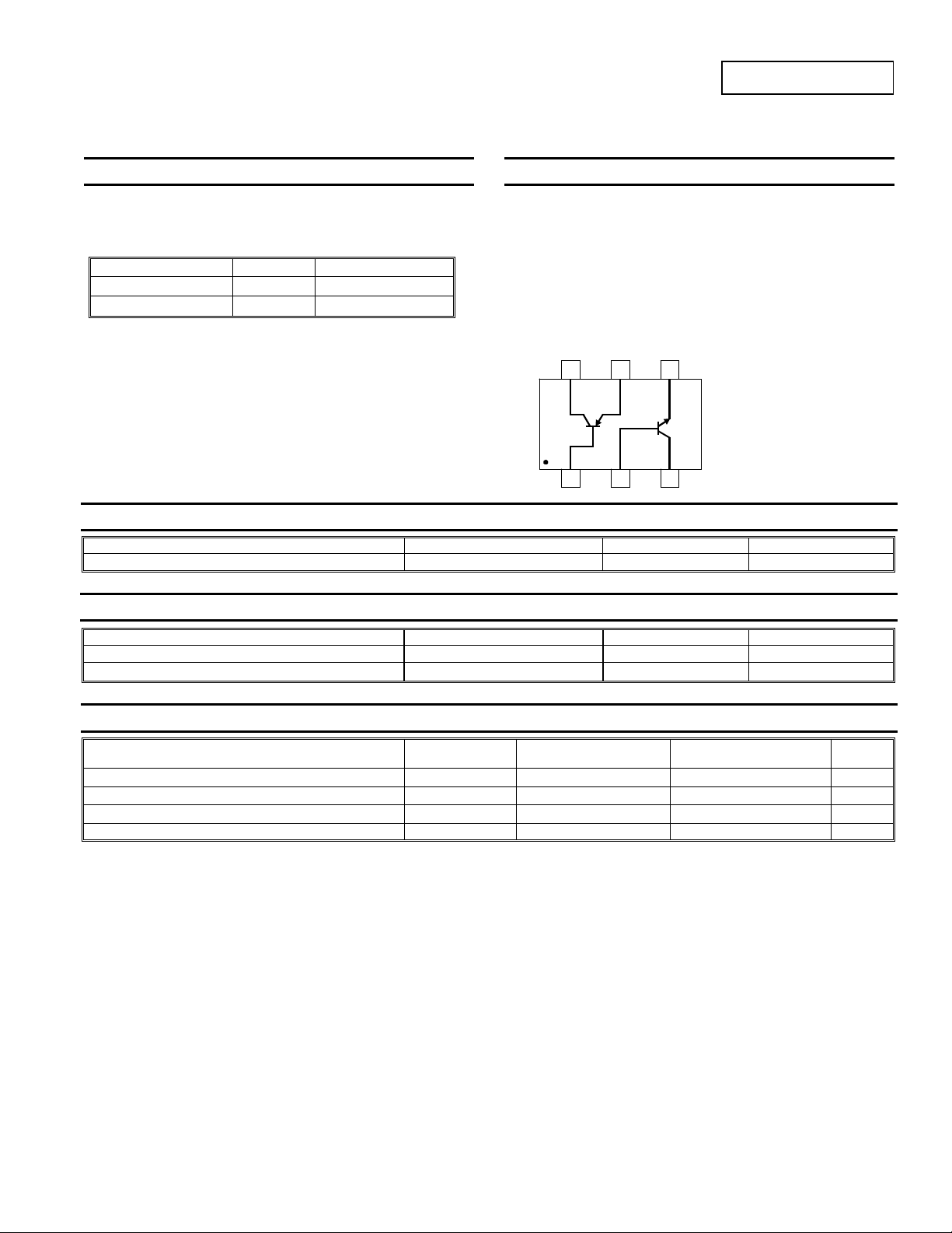
Sub-Component P/N Reference Device Type
MMBT2907A_DIE Q1 PNP Transistor
MMBTA06_DIE Q2 NPN Transistor
Top View
Maximum Ratings: Total Device @T
Characteristic Symbol Value Unit
Operating and Storage Junction Temperature Range
COMPLEX TRANSISTOR ARRAY FOR BIPOLAR
TRANSISTOR HALF H-BRIDGE MOTOR/ACTUATOR DRIVER
Mechanical Data
• Case: SOT-363
• Case Material: Molded Plastic, “Green” Molding Compound. UL
Flammability Classification Rating 94V-0
• Moisture Sensitivity: Level 1 per J-STD-020D
• Terminal Connections: See Schematic & Pin Configuration
• Terminals: Finish - Matte Tin annealed over Alloy 42 leadframe.
Solderable per MIL-STD-202, Method 208
• Marking Information: See Page 6
• Ordering Information: See Page 6
• Weight: 0.016 grams (approximate)
CQ1
MMBT2907A
BQ1
= 25°C unless otherwise specified
A
V
EBO
EQ1
Q1
MMBTA06
BQ2
Device Schematic
HBDM60V600
EQ2
Q2
CQ2
-55 to +150 °C
Thermal Characteristics: Total Device
Characteristic Symbol Value Unit
Power Dissipation (Note 3)
Thermal Resistance, Junction to Ambient Air (Note 3)
Maximum Ratings: Sub-Component Devices @T
Characteristic Symbol
Collector-Base Voltage
Collector-Emitter Voltage
Emitter-Base Voltage
Collector Current - Continuous (Note 3)
Notes: 1. No purposefully added lead.
2. Diodes Inc.'s "Green" policy can be found on our website at http://www.diodes.com/products/lead_free/index.php.
3. Device mounted on FR-4 PCB, 1 inch x 0.85 inch x 0.062 inch; pad layout as shown on page 7 or on Diodes Inc. suggested pad layout document
AP02001, which can be found on our website at http://www.diodes.com/datasheets/ap02001.pdf.
HBDM60V600W
Document number: DS30701 Rev. 5 - 2
PD
R
JA
θ
= 25°C unless otherwise specified
A
Q1-PNP Transistor
V
CBO
V
CEO
V
EBO
IC
1 of 7
www.diodes.com
200 mW
625 °C/W
Q2-NPN Transistor
(MMBT2907A)
-60 80 V
-60 65 V
-5.5 6 V
-600 500 mA
(MMBTA06)
© Diodes Incorporated
Unit
July 2008
Page 2
W
Electrical Characteristics: PNP (MMBT2907A) Transistor (Q1) @T
OFF CHARACTERISTICS (Note 4)
Collector-Base Breakdown Voltage
Collector-Emitter Breakdown Voltage
Emitter-Base Breakdown Voltage
Collector Cutoff Current
Collector Cutoff Current
Base Cutoff Current
ON CHARACTERISTICS (Note 4)
DC Current Gain
Collector-Emitter Saturation Voltage
Base-Emitter Saturation Voltage
SMALL SIGNAL CHARACTERISTICS
Current Gain-Bandwidth Product
SWITCHING CHARACTERISTICS
Turn-On Time
Delay Time
Rise Time
Turn-Off Time
Storage Time
Fall Time
Characteristic Symbol Min Max Unit Test Condition
V
(BR)CBO
V
(BR)CEO
V
(BR)EBO
I
CBO
I
CEX
I
⎯
BL
hFE
V
CE(SAT)
V
BE(SAT)
fT
t
⎯
on
t
⎯
d
t
⎯
r
t
⎯
off
t
⎯
s
t
⎯
r
-60
-60
-5.5
⎯
⎯
100
100
100
100
50
⎯
⎯
100
⎯
⎯
⎯
-10 nA
-50 nA
-50 nA
⎯
⎯
⎯
300
⎯
-0.3
-0.5
-0.95
-1.3
MHz
⎯
45 ns
10 ns
40 ns
100 ns
80 ns
30 ns
HBDM60V600
= 25°C unless otherwise specified
A
V
IC = -10μA, IE = 0
V
IC = -10mA, IB = 0
V
IE = -10μA, IC = 0
VCB = -50V, IE = 0
V
= -30V, V
CE
V
= -30V, V
CE
IC = -100μA, VCE = -10V
⎯
IC = -1.0mA, VCE = -10V
⎯
⎯
IC = -10mA, VCE = -10V
⎯
IC = -150mA, VCE = -10V
⎯
IC = -500mA, V
IC = -150mA, IB = -15mA
V
IC = -500mA, IB = -50mA
IC = -150mA, IB = -15mA
V
IC = -500mA, IB = -50mA
VCE = -2.0V, IC = -10mA,
f = 100MHz
= -30V, IC = -150mA,
V
CE
I
= -15mA
B1
= -6.0V, IC = -150mA,
V
CC
= I
= -15mA
I
B1
B2
EB(OFF)
EB(OFF)
= -10V
CE
= -0.5V
= -0.5V
Electrical Characteristics: NPN (MMBTA06) Transistor (Q2) @T
OFF CHARACTERISTICS (Note 4)
Collector-Base Breakdown Voltage
Collector-Emitter Breakdown Voltage
Emitter-Base Breakdown Voltage
Collector-Base Cutoff Current
Collector Cutoff Current
Emitter-Base Cutoff Current
ON CHARACTERISTICS (Note 4)
DC Current Gain
Collector-Emitter Saturation Voltage
Base-Emitter Turn-on Voltage
Base-Emitter Saturation Voltage
SMALL SIGNAL CHARACTERISTICS
Current Gain-Bandwidth Product
Notes: 4. Short duration pulse test used to minimize self-heating effect.
HBDM60V600W
Document number: DS30701 Rev. 5 - 2
Characteristic Symbol Min Typ Max Unit Test Condition
V
(BR)CBO
V
(BR)CEO
V
(BR)EBO
I
⎯ ⎯
CBO
I
⎯ ⎯
CES
I
⎯ ⎯
EBO
h
FE
V
CE(SAT)
V
BE(ON)
V
BE(SAT)
fT
80
65
6
250
100
⎯
0.7 0.75 0.8 V
⎯ ⎯
100
⎯ ⎯
⎯ ⎯
⎯ ⎯
⎯ ⎯ ⎯ V
⎯ ⎯ ⎯ V
0.2 0.4 V
0.95 V
⎯ ⎯
2 of 7
www.diodes.com
= 25°C unless otherwise specified
A
V
IC = 100μA, IE = 0
V
IC = 1mA, IB = 0
V
IE = 100μA, IC = 0
100 nA
100 nA
100 nA
VCB = 80V, IE = 0
V
= 90V, VBE = 0
CE
VEB = 5V, IC = 0
= 1V, IC = 10mA
CE
= 1V, IC = 100mA
CE
IC = 100mA, IB = 10mA
VCE = 1V, IC = 100mA
IC = 100mA, IB = 5mA
VCE = 20V, IC = 10mA,
MHz
f = 100MHz
July 2008
© Diodes Incorporated
Page 3
W
P, P
OWER
PATIO
N
C, CAPACITANC
F
C
O
CTO
R
T
TER VOLTAG
C
O
C
T
O
R T
O
T
T
R
C CUR
R
T
G
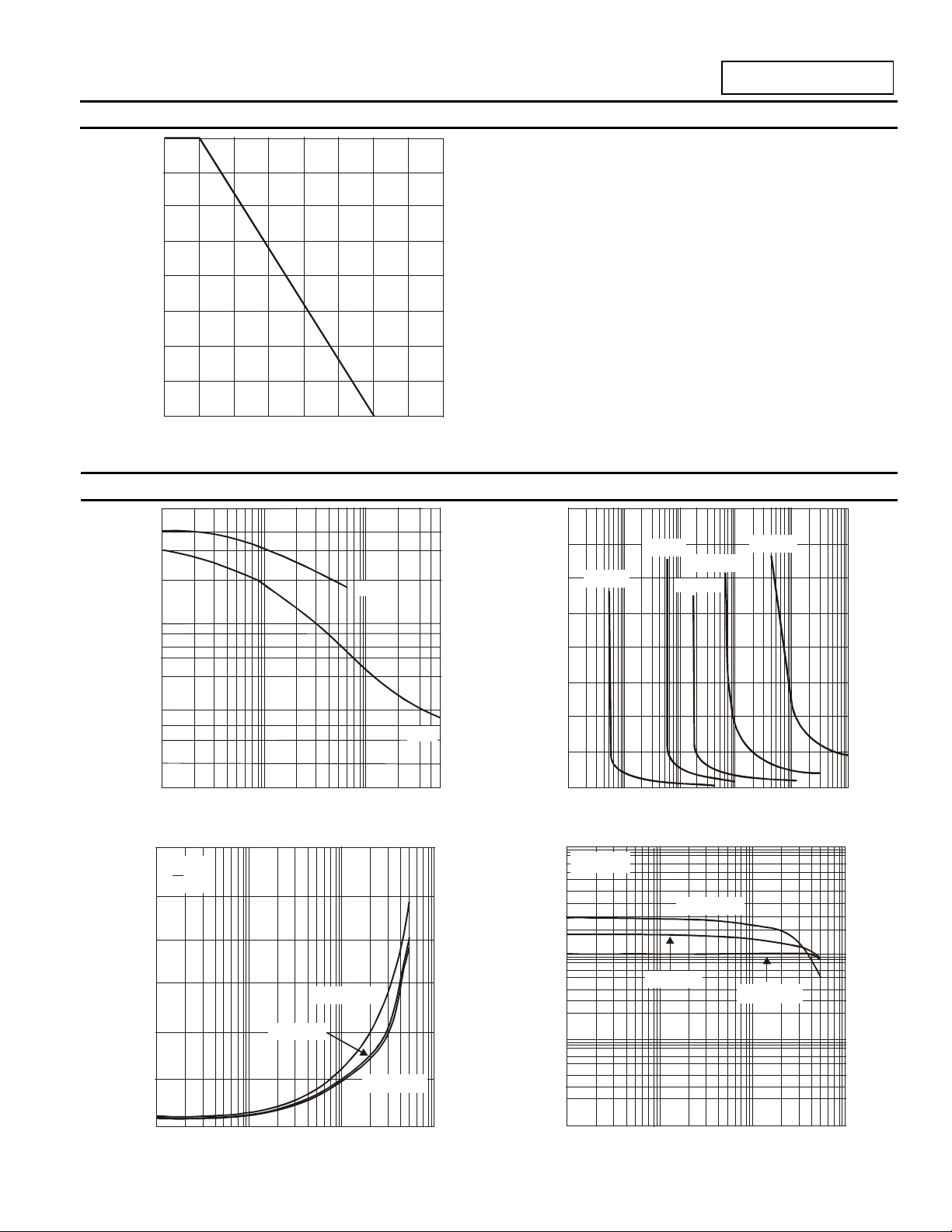
Typical Characteristics @T
= 25°C unless otherwise specified
A
200
150
(mW)
100
DISSI
50
D
0
0
25 50
T , AMBIENT TEMPERATURE (°C)
75 100 125
A
150
175
200
Fig. 1 Power Derating Curve
PNP (MMBT2907A) Transistor (Q1) Plots:
30
HBDM60V600
1.6
1
T = -50°C
I = 300mA
C
10 100
A
1.4
20
10
)
Cibo
E (p
5.0
Cobo
1.0
0.1
1.0 30
10
E (V)
1.2
1.0
0.8
-EMI
0.6
LLE
0.4
CE
0.2
-V ,
0
0.001 0.01
I = 1mA
C
REVERSE VOLTAGE (V)
Fig. 2 Typical Capacitance
0.6
I
C
= 10
I
0.5
0.4
0.3
B
T = 150°C
A
E
EMI
1,000
V = 5V
CE
AIN
100
EN
I = 10mA
C
I = 100mA
C
I = 30mA
C
0.1
-I , BASE CURRENT (mA)
B
Fig. 3 Typical Collector Saturation Region
T = 150°C
A
T = 25°C
A
LLE
0.2
SATURATION VOLTAGE (V)
CE(SAT)
0.1
-V ,
T = 25°C
A
T = -50°C
A
FE
h, D
10
0
110
-I , COLLECTOR CURRENT (mA)
C
100
Fig. 4 Collector Emitter Saturation Voltage vs. Collector Current
HBDM60V600W
Document number: DS30701 Rev. 5 - 2
1,000
3 of 7
www.diodes.com
1
110
-I , COLLECTOR CURRENT (mA)
C
100
Fig. 5 Typical DC Current Gain vs. Collector Current
© Diodes Incorporated
1,000
July 2008
Page 4

W
T
TER VO
TAG
G
T
H P
R
ODU
C
T
H
C
O
CTO
R
T
TER VOLTAG
C
C
URR
T
G
C
O
CTO
R T
O
T
TER
1.0
V = 5V
CE
0.9
E (V)
T = -50°C
0.8
L
A
0.7
0.6
T = 25°C
A
0.5
0.4
BE(ON)
-V , BASE EMI
0.3
T = 150°C
A
0.2
0.1
110
-I , COLLECTOR CURRENT (mA)
C
100
Fig. 6 Typical Base Emitter Voltag e vs. C ollector Cur rent
NPN (MMBTA06) Transistor (Q2) Plots
10
HBDM60V600
1,000
z)
(M
100
10
AIN BANDWID
T
f,
1
1
-I , COLLECTOR CURRENT (mA)
Fig. 7 Typical Gain Bandwidth Product vs. Collector Current
C
2.0
1.8
E (V)
1.6
10 100
1
0.1
CBO
I , COLLECTOR-BASE CURRENT (nA)
0.01
25 50 75 100 125
T , AMBIENT TEMPERATURE (ºC)
A
Fig. 8 Typical C ol lector-Cuto f f Current vs . Ambien t Tempera
0.500
I
0.450
C
= 10
I
B
0.400
EMI
0.350
0.300
T = 25°C
A
0.250
T = 150°C
LLE
0.200
A
ture
1.4
I = 30mA
1.2
1.0
EMI
I = 10mA
C
C
0.8
LLE
CE
V,
0.6
0.4
0.2
I = 1mA
C
I = 100mA
C
0
0.001 0.01
Fig. 9 Typical Collector Saturation Region
0.1
I BASE CURRENT (mA)
B,
1
10 100
10,000
1,000
AIN
EN
100
0.150
SATURATION VOLTAGE (V)
CE(SAT)
0.100
V,
0.050
0
110
I , COLLECTOR CURRENT (mA)
C
100
T = -50°C
A
1,000
Fig. 10 Typical Collector Emitter Saturation Voltage vs. Collector Current
HBDM60V600W
Document number: DS30701 Rev. 5 - 2
4 of 7
www.diodes.com
FE
h, D
10
1
1
10
I , COLLECTOR CURRENT (mA)
C
100
Fig. 11 T y pical DC Current Gain vs. Collector Curren
1,000
t
July 2008
© Diodes Incorporated
Page 5

W
G
T
H PRODUCT
H
T
TER VO
T
G
1.0
0.9
E (V)
0.8
A
L
0.7
1,000
z)
(M
100
0.6
0.5
0.4
0.3
BE(ON)
V , BASE EMI
0.2
AIN BANDWID
T
f,
0.1
0.1
110
I , COLLECTOR CURRENT (mA)
C
Fig. 12 Typical Base Emitter Voltage vs. Collector Current
100
Fig. 13 Typical Gain Bandwidth Product vs. Collector Current
Current Schematic along with Application Example:
9V-12V
10
HBDM60V600
1
1
I , COLLECTOR CURRENT (mA)
C
10
HBDM60V600W
EQ1
MMBT2907A
R5
1k
R3
Q3
Half H-Bridge
Q1
BQ1
CQ1
CQ2
MMBTA06
Q2
BQ2
D1
D3
Forward
Note: D1, D2, D3, D4: Switching Diodes (MMBD4448)
Q3, Q4: NPN Transistors (MMBTA06)
R1
C1
0
Motor
C2
EQ2
0
HBDM60V600W
MMBT2907A
Q1
D2
BQ1
CQ1
Half H-Bridge
CQ2
MMBTA06
Q2
D4
BQ2
R4
Q4
R8
1k
Reverse
36
HBDM60V600W
Document number: DS30701 Rev. 5 - 2
5 of 7
www.diodes.com
July 2008
© Diodes Incorporated
Page 6

W
W
Application Example Schematic: (with Package Pinouts)
Application Example Schematic: (with Package Pinouts)
U1
U1
A1
A1
1
NC
NC
2
C2
C2
34
MMBD4448DW
MMBD4448DW
U4
U4
BQ1
R4
R4
470
470
R6
1k
Q1
BQ1
1
1
BQ2
BQ2
2
2
CQ2
CQ2
34
34
HBDM60V600W
HBDM60V600W
6
6
5
5
CQ1
CQ1
EQ1
EQ1
EQ2
EQ2
Motor
C2
U5
U5
A1
A1
1
1
A2
A2
2
2
A3 C3
A3 C3
34
34
MMMBD4448HTW
MBD4448HTW
6
5
6
6
5
5
9V-12V
C1
NC
A2
A2
C1
C1
C2
C2
R1
R1
36
36
C1
U2
BQ1
1
BQ2
2
CQ2
34
HBDM60V600W
Forward
6
5
CQ1
EQ1
EQ2
R3
R3
470
470
U3
U3
EQ1
EQ1
1
1
BQ2
BQ2
2
2
CQ2
CQ2
34
34
INV5V0W
INV5V0W
R5
1k
Reverse
Reverse
HBDM60V600
HBDM60V600
R2
R2
33k
33k
CQ1
CQ1
6
6
BQ1
BQ1
5
5
EQ2
EQ2
Control Input 5V/0V
Control Input 5V/0V
Ordering Information (Note 5)
Part Number Case Packaging
HBDM60V600W-7 SOT-363 3000/Tape & Reel
Notes: 5. For packaging details, go to our website at http://www.diodes.com/datasheets/ap02007.pdf.
Marking Information
HB01
Date Code Key
Year 2006 2007 2008 2009 2010 2011 2012 2013 2014 2015
Code T U V W X Y Z A B C
Month Jan Feb Mar Apr May Jun Jul Aug Sep Oct Nov Dec
Code 1 2 3 4 5 6 7 8 9 O N D
HBDM60V600W
HBDM60V600W
Document number: DS30701 Rev. 5 - 2
Document number: DS30701 Rev. 5 - 2
www.diodes.com
www.diodes.com
HB01 = Product Type Marking Code
YM = Date Code Marking
Y = Year (ex: T = 2006)
YM
M = Month (ex: 9 = September)
6 of 7
6 of 7
© Diodes Incorporated
© Diodes Incorporated
July 2008
July 2008
Page 7

W
HBDM60V600
Package Outline Dimensions
K
J
A
SOT-363
Dim Min Max
B C
H
M
D
L
F
A 0.10 0.30
B 1.15 1.35
C 2.00 2.20
D 0.65 Typ
F 0.40 0.45
H 1.80 2.20
J 0 0.10
K 0.90 1.00
L 0.25 0.40
M 0.10 0.22
α
All Dimensions in mm
0° 8°
Suggested Pad Layout
Diodes Incorporated and its subsidiaries reserve the right to make modifications, enhancements, improvements, corrections or other changes
without further notice to any product herein. Diodes Incorporated does not assume any liability arising out of the application or use of any product
described herein; ghts of others. The user of products in such applications shall neither does it convey any license under its patent rights, nor the ri
assume all risks of such rporated a are represented on our website, use and will agree to hold Diodes Inco nd all the companies whose products
harmless against all damages.
Diodes Incorporated pro al compo ystems without the expressed written ducts are not authorized for use as critic nents in life support devices or s
approval of the President of Diodes Incorporated.
G
Z
Y
X
E E
Dimensions Value (in mm)
C
IMPORTANT NOTICE
LIFE SUPPORT
Z 2.5
G 1.3
X 0.42
Y 0.6
C 1.9
E 0.65
HBDM60V600W
Document number: DS30701 Rev
. 5 - 2
7 of 7
www.diod
es.com
July 2008
© Diodes Incorporated
 Loading...