

Page 1
)
(AV)
θ
Pb
GBU10005 - GBU1010
10A GLASS PASSIVATED BRIDGE RECTIFIER
Features
• Glass Passivated Die Construction
• High Case Dielectric Strength of 1500V
• Low Reverse Leakage Current
• Surge Overload Rating to 220A Peak
• Ideal for Printed Circuit Board Applications
• UL Listed Under Recognized Component
Index, File Number E94661
• Lead-Free Finish; RoHS Compliant (Notes 1 & 2)
RMS
Mechanical Data
• Case: GBU
• Case Material: Molded Plastic. UL Flammability Classification
Rating 94V-0
• Moisture Sensitivity: Level 1 per J-STD-020
• Terminals: Matte Tin Finish. Solderable per MIL-STD 202, Method
• Polarity: Marked on Body
• Mounting: Through Hole for #6 Screw
• Mounting Torque: 5.0 Inch-pounds Maximum
• Marking: Date Code and Type Number
• Weight: 4 grams (approximate)
208
Ordering Information (Note 3)
Part Number Case Packaging
GBU10005-GBU1010 GBU 20/Tube
Notes: 1. EU Directive 2002/95/EC (RoHS) & 2011/65/EU (RoHS 2) compliant. All applicable RoHS exemptions applied.
2. See http://www.diodes.com for more information about Diodes Incorporated’s definitions of Halogen- and Antimony-free, "Green" and Lead-free.
3. For packaging details, go to our website at http://www.diodes.com.
Maximum Ratings and Electrical Characteristics (@T
Single phase, half wave, 60Hz, resistive or inductive load.
For capacitive load, derate current by 20%.
Characteristic Symbol
Peak Repetitive Reverse Voltage
Working Peak Reverse Voltage
DC Blocking Voltage
RMS Reverse Voltage
Average Forward Rectified Current (Note 4) @ TC = +100°C I
Non-Repetitive Peak Forward Surge Current
8.3ms Single Half Sine-Wave Superimposed on Rated Load
Forward Voltage (per element) @ IF = 5.0A VFM
@ T
@ T
= +25°C
C
= +125°C
C
Peak Reverse Current at
Rated DC Blocking Voltage
I2t Rating for Fusing (Note 5) I2t
Typical Total Capacitance per Element (Note 6)
Typical Thermal Resistance Junction to Case (Note 4)
Operating and Storage Temperature Range
Notes: 4. Unit mounted on 100mm x 100mm x 1.6mm copper plate heatsink.
5. Non-repetitive, for t > 1.0ms and < 8.3ms.
6. Measured at 1.0MHz and applied reverse voltage of 4.0V DC.
GBU10005 - GBU1010
Document number: DS30052 Rev. 6 - 2
V
RRM
V
RWM
V
R
V
R(RMS
I
FSM
I
R
C
T
R
JC
T
J, TSTG
1 of 4
www.diodes.com
= +25°C, unless otherwise specified.)
A
GBU
10005
GBU
1001
50 100 200 400 600 800 1000 V
35 70 140 280 420 560 700 V
GBU
1002
GBU
1004
-55 to +150
GBU
1006
10 A
220 A
1.0 V
5.0
500
200
60 pF
2.2
GBU
1008
November 2012
© Diodes Incorporated
GBU
1010
Unit
μA
A2s
°C/W
°C
Page 2
G F
O
R
RD REC
TIF
CUR
REN
T
NSTAN
TANEO
US FORWAR
C
URREN
T
P
FORWAR
URGE CUR
REN
T
C, TOT
CAPACITANC
F
GBU10005 - GBU1010
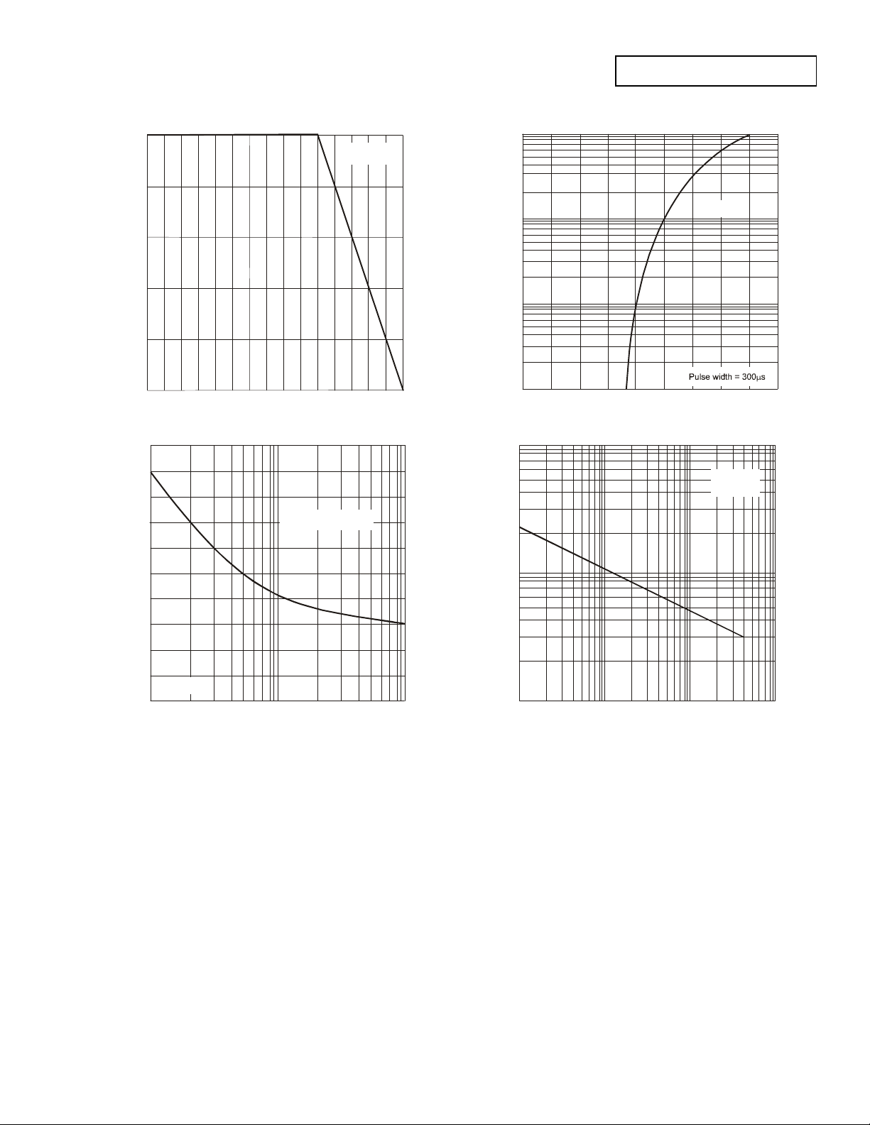
10
(A)
Resistive or
Inductive Load
100
(A)
8
T = 25C
°
D
IED
6
10
J
4
WA
1.0
2
(AV)
I, AV
0
050100150
T , CASE TEMPERATURE ( C)
C
°
Figure 1 Forward Current Derating Curve
250
(A)
200
Single half-sine wave
F
I, I
0.1
0.20 0.6 1.0 1.8
V , INSTANTANEOUS FORWARD VOLTAGE (V)
F
1.4
Figure 2 Typical Forward Characteristics, per element
1,000
T = 25C
)
f = 1.0MHz
E (p
°
J
150
D S
100
100
AL
50
EAK
T = 25C
°
FSM
I,
J
0
110100
NUMBER OF CYCLES AT 60Hz
Figure 3 Maximum Non-Repetitive Surge Current
T
10
0.1 1.0 10 100
V , REVERSE VOLTAGE (V)
R
Figure 4 Typical Total Capacitance, per element
GBU10005 - GBU1010
Document number: DS30052 Rev. 6 - 2
2 of 4
www.diodes.com
November 2012
© Diodes Incorporated
Page 3

Package Outline Dimensions
Please see AP02002 at http://www.diodes.com/datasheets/ap02002.pdf for latest version.
L
J
A
K
B
C
O
~
-
~
H
D
+
E
F
G
M
N
P
GBU10005 - GBU1010
Dim Min Max
All Dimensions in mm
GBU
A 21.8 22.3
B 3.5 4.1
C 7.4 7.9
D 1.65 2.16
E 2.25 2.75
F 1.95 2.35
G 1.02 1.27
H 4.83 5.33
J 17.5 18.0
K
L 18.3 18.8
M 3.30 3.56
N 0.46 0.56
O 1.90R
P 0.76 1.0
3.2 X 45°
GBU10005 - GBU1010
Document number: DS30052 Rev. 6 - 2
3 of 4
www.diodes.com
November 2012
© Diodes Incorporated
Page 4

IMPORTANT NOTICE
DIODES INCORPORATED MAKES NO WARRANTY OF ANY KIND, EXPRESS OR IMPLIED, WITH REGARDS TO THIS DOCUMENT,
INCLUDING, BUT NOT LIMITED TO, THE IMPLIED WARRANTIES OF MERCHANTABILITY AND FITNESS FOR A PARTICULAR PURPOSE
(AND THEIR EQUIVALENTS UNDER THE LAWS OF ANY JURISDICTION).
Diodes Incorporated and its subsidiaries reserve the right to make modifications, enhancements, improvements, corrections or other changes
without further notice to this document and any product described herein. Diodes Incorporated does not assume any liability arising out of the
application or use of this document or any product described herein; neither does Diodes Incorporated convey any license under its patent or
trademark rights, nor the rights of others. Any Customer or user of this document or products described herein in such applications shall assume
all risks of such use and will agree to hold Diodes Incorporated and all the companies whose products are represented on Diodes Incorporated
website, harmless against all damages.
Diodes Incorporated does not warrant or accept any liability whatsoever in respect of any products purchased through unauthorized sales channel.
Should Customers purchase or use Diodes Incorporated products for any unintended or unauthorize d application, Customers shall indemnify and
hold Diodes Incorporated and its representatives harmless against all claims, damages, expenses, and attorney fees arising out of, directly or
indirectly, any claim of personal injury or death associated with such unintended or unauthorized application.
Products described herein may be covered by one or more United States, international or foreign patents pending. Product names and markings
noted herein may also be covered by one or more United States, international or foreign trademarks.
This document is written in English but may be translated into multiple languages for reference. Onl y the English version of this document is the
final and determinative format released by Diodes Incorporated.
LIFE SUPPORT
Diodes Incorporated products are specifically not authorized for use as critical components in life support devices or systems without the express
written approval of the Chief Executive Officer of Diodes Incorporated. As used herein:
A. Life support devices or systems are devices or systems which:
1. are intended to implant into the body, or
2. support or sustain life and whose failure to perform when properly used in accordance with instructions for use provided in the
labeling can be reasonably expected to result in significant injury to the user.
B. A critical component is any component in a life support device or system whose failure to perform can be reasonably expected to cause the
failure of the life support device or to affect its safety or effectiveness.
Customers represent that they have all necessary expertise in the safety and regulatory ramifications of their life support devices or systems, and
acknowledge and agree that they are solely responsible for all legal, regulatory and safety-related requirements concerning their products and any
use of Diodes Incorporated products in such safety-critical, life support devices or systems, notwithstanding any devices- or systems-related
information or support that may be provided by Diodes Incorporated. Further, Customers must fully indemnify Diodes Incorporated and its
representatives against any damages arising out of the use of Diodes Incorporated products in such safety-critical, life support devices or systems.
Copyright © 2012, Diodes Incorporated
www.diodes.com
GBU10005 - GBU1010
GBU10005 - GBU1010
Document number: DS30052 Rev. 6 - 2
4 of 4
www.diodes.com
November 2012
© Diodes Incorporated
 Loading...