Diodes FZT956 User Manual

A
f
y
B
Product Line o
Green
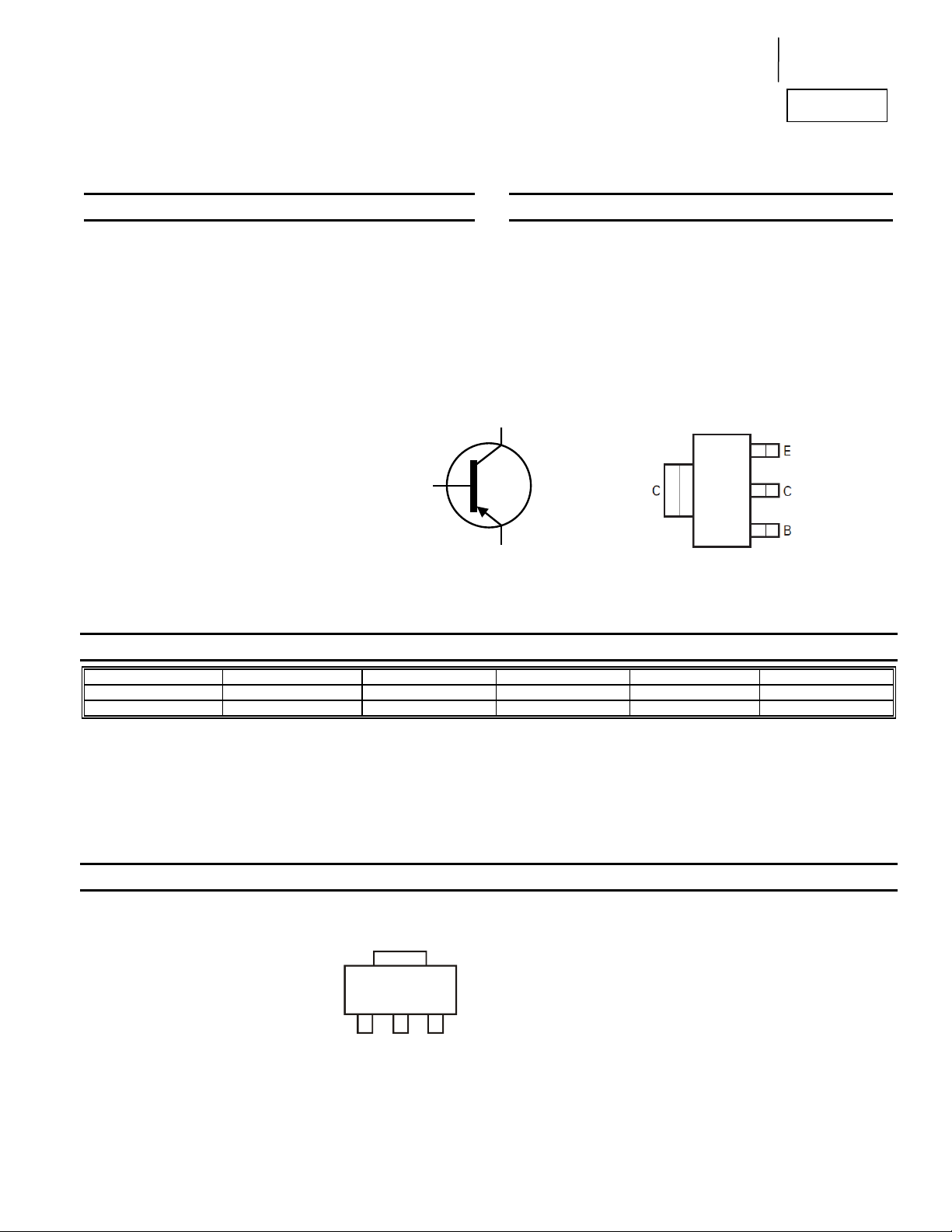
200V PNP SILICON PLANAR MEDIUM POWER TRANSISTOR IN SOT223
Features
• BV
• I
• I
• Low Saturation Voltage V
• h
• Lead-Free Finish; RoHS Compliant (Notes 1 & 2)
• Halogen and Antimony Free. “Green” Device (Note 3)
• Qualified to AEC-Q101 Standards for High Reliability
• PPAP capable (Note 4)
> -200V
CEO
= -2A high Continuous Collector Current
C
= -5A Peak Pulse Current
C
specified up to -5A for a high gain hold up
FE
SOT223
Top View
< -165mV @ -1A
CE(sat)
Device S
Mechanical Data
• Case: SOT223
• Case material: molded plastic. “Green” molding compound.
• UL Flammability Rating 94V-0
• Moisture Sensitivity: Level 1 per J-STD-020
• Terminals: Finish - Matte Tin Plated Leads, Solderable per
MIL-STD-202, Method 208
• Weight: 0.112 grams (approximate)
C
E
mbol
Diodes Incorporated
FZT956
Top View
Pin-Out
Ordering Information (Notes 4 & 5)
Product Compliance Marking Reel size (inches) Tape width (mm) Quantity per reel
FZT956TA AEC-Q101 FZT956 7 12 1,000
FZT956QTA Automotive FZT956 7 12 1,000
Notes: 1. EU Directive 2002/95/EC (RoHS) & 2011/65/EU (RoHS 2) compliant. All applicable RoHS exemptions applied.
2. See http://www.diodes.com for more information about Diodes Incorporated’s definitions of Halogen- and Antimony-free, "Green" and Lead-free.
3. Halogen- and Antimony-free "Green” products are defined as those which contain <900ppm bromine, <900ppm chlorine (<1500ppm total Br + Cl) and
<1000ppm antimony compounds.
4. Automotive products are AEC-Q101 qualified and are PPAP capable. Automotive, AEC-Q101 and standard products are electrically and thermally
the same, except where specified.
5. For packaging details, go to our website at http://www.diodes.com.
Marking Information
FZT956
tasheet Number: DS36119 Rev. 4 - 2
Da
FZT
956
FZT956 = Product Type Marking Code
1 of 7
www.diodes.com
November 2012
© Diodes Incorporated

A
f
θ
θ
θ
Product Line o
Diodes Incorporated
FZT956
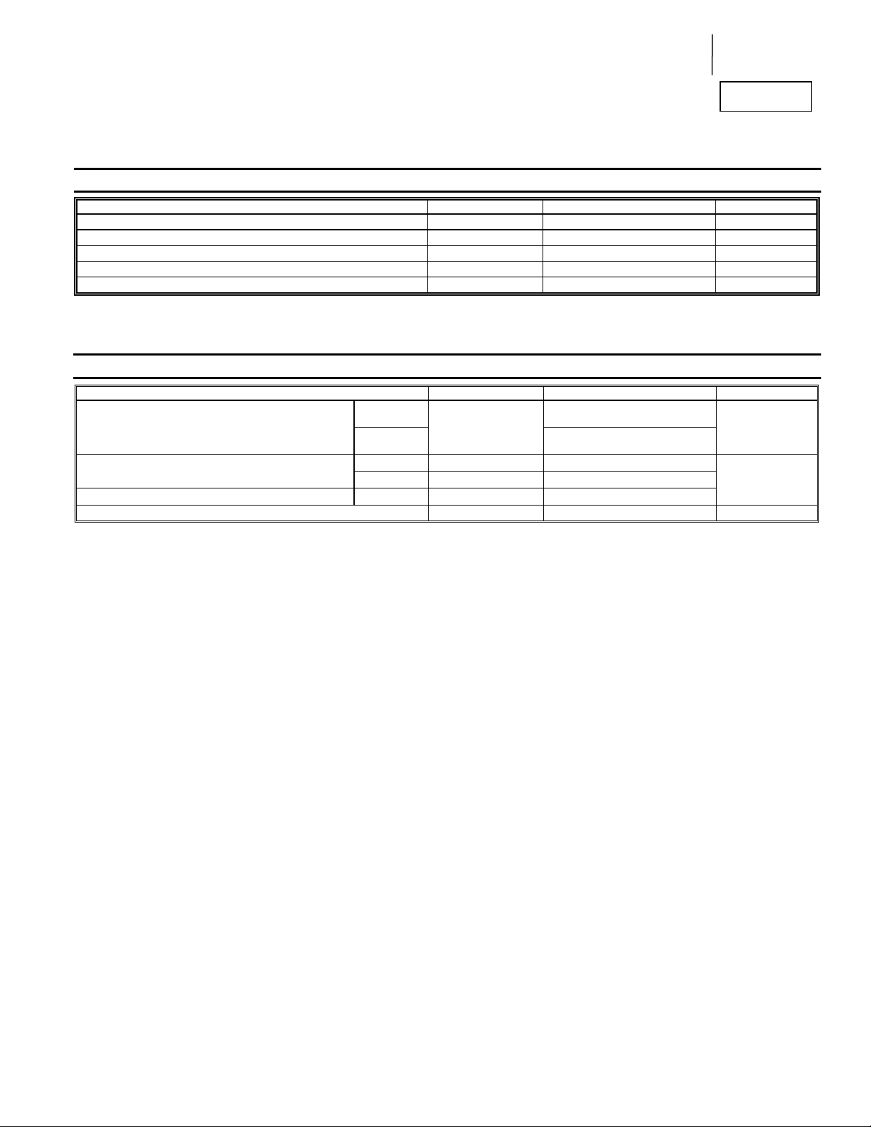
Maximum Ratings (@T
= +25°C, unless otherwise specified.)
A
Characteristic Symbol Value Unit
Collector-Base Voltage
Collector-Emitter Voltage
Emitter-Base Voltage
Continuous Collector Current
Peak Pulse Current
V
CBO
V
CEO
V
EBO
I
C
I
CM
-220 V
-200 V
-7 V
-2 A
-5 A
Thermal Characteristics (@T
= +25°C, unless otherwise specified.)
A
Characteristic Symbol Value Unit
Power Dissipation
Linear derating factor
Thermal Resistance, Junction to Ambient
Thermal Resistance Junction to Lead (Note 8)
Operating and Storage Temperature Range
Notes: 6. For a device surface mounted on 52mm x 52mm x 1.6mm FR4 PCB with high coverage of single sided 2oz copper, in still air conditions; the device is
measured when operating in a steady-state condition.
7. Same as note (6), except the device is surface mounted on 25mm x 25mm with 1oz copper.
8. Thermal resistance from junction to solder-point (at the end of the collector lead).
(Note 6)
(Note 7)
(Note 6)
(Note 7)
P
R
R
R
T
J, TSTG
D
JA
JA
JL
3.0
24
1.6
12.8
42
78
8.84
-55 to +150
W
mW /°C
°C/W
°C
FZT956
tasheet Number: DS36119 Rev. 4 - 2
Da
2 of 7
www.diodes.com
November 2012
© Diodes Incorporated

A
f
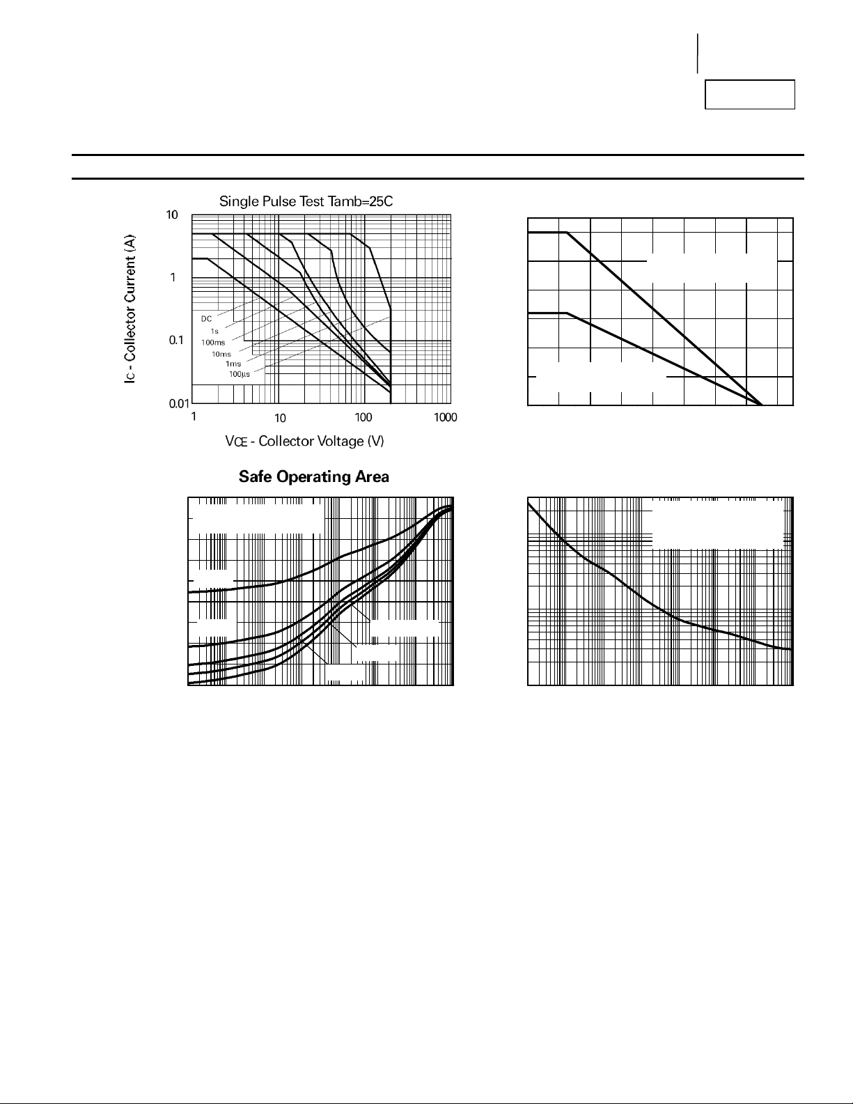
Thermal Characteristics and Derating Information
Product Line o
Diodes Incorporated
FZT956
V
CE(sat)
10
Limit
1
DC
1s
100m
100ms
Single Pulse. T
Collector Current (A)
C
10m
-I
100m 1 10 100
52mmX52mm
single sided 2oz Cu
amb
10ms
=25°C
1ms
100µs
-VCE Collector-Emitter Voltage (V)
Safe Operating Area
52mm X52mm
40
single sided 2oz Cu
30
D=0.5
20
D=0.2
10
0
100µ 1m 10m 100m 1 10 100 1k
Thermal Resistance (°C/W)
Pulse Width (s)
Single Pulse
D=0.05
D=0.1
Transient Thermal Impedance
3.0
2.5
52mm X52mm
single sided 2oz Cu
2.0
1.5
1.0
25mm X25mm
0.5
single sided 1oz Cu
0.0
0 20 40 60 80 100 120 140 160
Max Powe r D i ssipation (W )
Temperature (°C)
Derating Curve
Single Pulse. T
100
52mmX52mm
single sided 2oz Cu
10
1
100µ 1m 10m 100m 1 10 100 1k
Max Power Dissipation (W)
Pulse Width (s)
amb
Pulse Power Dissipation
=25°C
3 of 7
November 2012
© Diodes Incorporated
FZT956
tasheet Number: DS36119 Rev. 4 - 2
Da
www.diodes.com
 Loading...