Diodes FZT651Q User Manual

A
f
y
Product Line o
Green
60V NPN HIGH PERFORMANCE TRANSISTOR IN SOT223
Description
Mechanical Data
Diodes Incorporated
FZT651Q
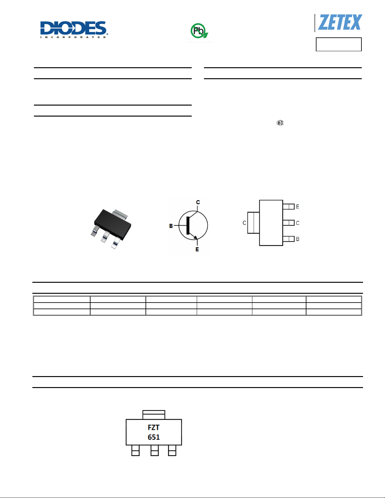
This Bipolar Junction Transistor (BJT) has been designed to meet the
stringent requirements of Automotive Applications.
Features
• BV
• I
• I
• Low Saturation Voltage V
• Complementary PNP Type: FZT751Q
• Lead-Free Finish; RoHS compliant (Notes 1 & 2)
• Halogen and Antimony Free. “Green” Device (Note 3)
• Qualified to AEC-Q101 Standards for High Reliability
• PPAP Capable (Note 4)
> 60V
CEO
= 3A High Continuous Current
C
= 6A Peak Pulse Current
CM
CE(sat)
Top View
< 300mV @ 1A
SOT223
Device S
• Case: SOT223
• Case material: molded plastic. “Green” molding compound.
• UL Flammability Rating 94V-0
• Moisture Sensitivity: Level 1 per J-STD-020
• Terminals: Finish - Matte Tin Plated Leads, Solderable per
MIL-STD-202, Method 208
• Weight: 0.112 grams (approximate)
mbol
Top View
Pin-Out
Ordering Information (Notes 4 & 5)
Product Compliance Marking Reel size (inches) Tape width (mm) Quantity per reel
FZT651QTA Automotive FZT651 7 12 1,000
FZT651QTC Automotive FZT651 13 12 4,000
Notes: 1. EU Directive 2002/95/EC (RoHS) & 2011/65/EU (RoHS 2) compliant. All applicable RoHS exemptions applied.
2. See http://www.diodes.com/quality/lead_free.html for more information about Diodes Incorporated’s definitions of Halogen- and Antimony-free, "Green"
and Lead-free.
3. Halogen- and Antimony-free "Green” products are defined as those which contain <900ppm bromine, <900ppm chlorine (<1500ppm total Br + Cl) and
<1000ppm antimony compounds.
4. Automotive products are AEC-Q101 qualified and are PPAP capable. Automotive, AEC-Q101 and standard products are electrically and thermally
the same, except where specified. For more information, please refer to http://www.diodes.com/quality/product_compliance_definitions/.
5. For packaging details, go to our website at http://www.diodes.com/products/packages.html
Marking Information
FZT651 = Product Type Marking Code
FZT651Q
Document Number DS36917 Rev. 1 - 2
1 of 7
www.diodes.com
February 2014
© Diodes Incorporated

A
f
Absolute Maximum Ratings (@T
Characteristic Symbol Value Unit
Collector-Base Voltage
Collector-Emitter Voltage
Emitter-Base Voltage
Continuous Collector Current
Peak Pulse Current
= +25°C, unless otherwise specified.)
A
V
CBO
V
CEO
V
EBO
I
C
I
CM
Product Line o
Diodes Incorporated
FZT651Q
80 V
60 V
7 V
3 A
6 A
Thermal Characteristics (@T
Characteristic Symbol Value Unit
Power Dissipation
Thermal Resistance, Junction to Ambient
Thermal Resistance, Junction to Leads (Note 8)
Operating and Storage Temperature Range
= +25°C, unless otherwise specified.)
A
(Note 6)
(Note 7) 3 W
(Note 6)
(Note 7) 41.7
P
R
R
T
J, TSTG
θJA
θJL
D
2 W
62.5
12.9
-55 to +150
°C/W
°C/W
°C/W
°C
ESD Ratings (Note 9)
Characteristic Symbol Value Unit JEDEC Class
Electrostatic Discharge - Human Body Model ESD HBM 4,000 V 3a
Electrostatic Discharge - Machine Model ESD MM 400 V C
Notes: 6. For a device mounted with the collector lead on 25mm x 25mm 2oz copper that is on a single-sided 1.6mm FR4 PCB; device is measured under still air
8. Thermal resistance from junction to solder-point (at the end of the collector lead).
9. Refer to JEDEC specification JESD22-A114 and JESD22-A115.
conditions whilst operating in steady-state.
7. Same as note (6), except the device is mounted on 50mm x 50mm 2oz copper.
FZT651Q
Document Number DS36917 Rev. 1 - 2
2 of 7
www.diodes.com
February 2014
© Diodes Incorporated

A
f
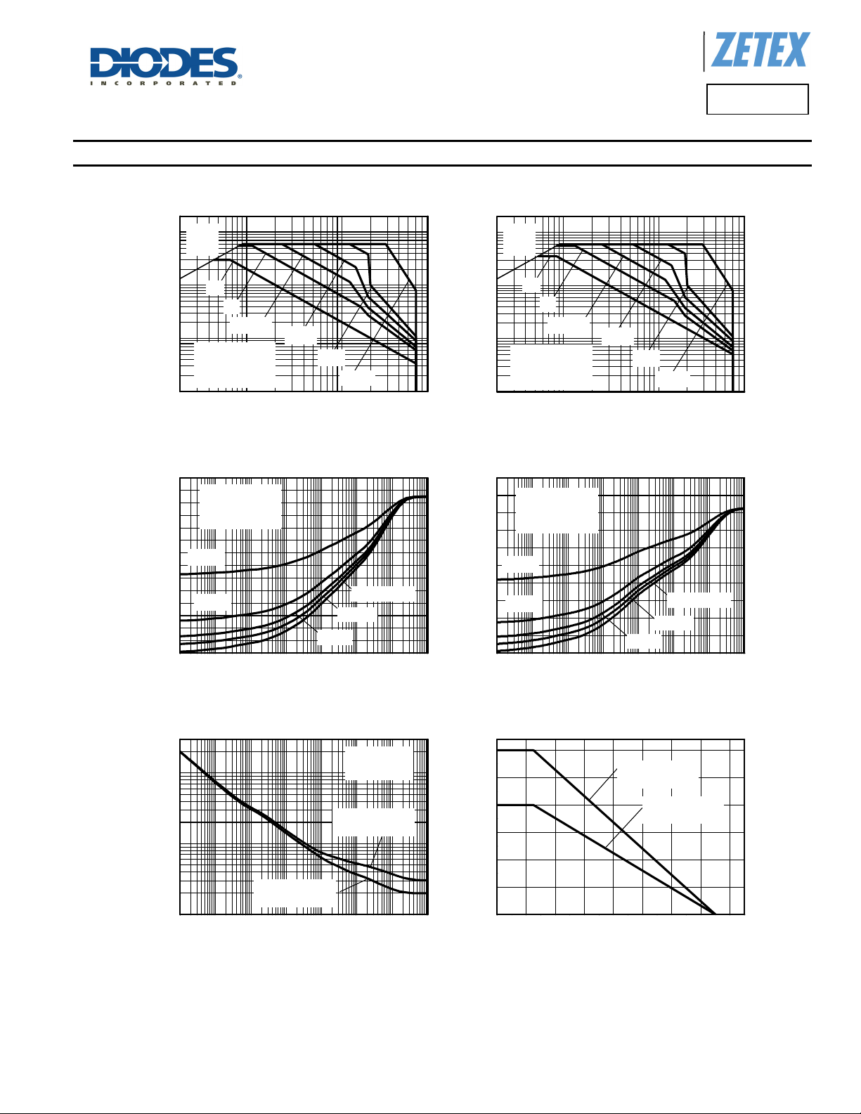
Thermal Characteristics and Derating Information
V
10
CE(sat)
Limit
10
V
CE(sat)
Limit
Product Line o
Diodes Incorporated
FZT651Q
1
DC
1s
100m
Collector Current (A)
C
I
10m
100ms
T
=25°C
amb
25mm x 25mm
2oz FR4
110
10ms
1ms
100µs
VCE Collector-Emitter Voltage (V)
Safe Operating Area
70
T
=25°C
60
50
40
30
20
10
0
100µ 1m 10m 100m 1 10 100 1k
Thermal Resistance (°C/W)
amb
25mm x 25mm
2oz FR4
D=0.5
D=0.2
Single Pulse
D=0.05
D=0.1
Pulse Width (s)
Transient Thermal Impedance
1
DC
1s
100m
Collector Current (A)
C
10m
I
100ms
T
=25°C
amb
50mm x 50mm
2oz FR4
110
10ms
1ms
100µs
VCE Collector-Emitter Voltage (V)
Safe Operating Area
50
T
=25°C
40
30
20
10
0
100µ 1m 10m 100m 1 10 100 1k
Thermal Resistance (°C/W)
amb
50mm x 50mm
2oz FR4
D=0.5
D=0.2
Single Pulse
D=0.05
D=0.1
Pulse Width (s)
Transient Thermal Impedance
Single Pulse
T
=25°C
100
10
25mm x 25mm
1
100µ 1m 10m 100m 1 10 100 1k
Max Power Dissipation (W)
2oz FR4
Pulse Width (s)
amb
50mm x 50mm
2oz FR4
Pulse Power Dissipation
FZT651Q
Document Number DS36917 Rev. 1 - 2
3 of 7
www.diodes.com
3.0
2.5
2.0
1.5
1.0
0.5
0.0
0 20 40 60 80 100 120 140 160
Max Power Dissipation (W)
Temperature (°C)
50mm x 50mm
2oz FR4
25mm x 25mm
2oz FR4
Derating Curve
February 2014
© Diodes Incorporated
 Loading...