Diodes FZT605 User Manual

A
f
y
605
Product Line o
Green
120V NPN DARLINGTON TRANSISTOR IN SOT223
Features
Mechanical Data
Diodes Incorporated
FZT605
BV
BV
I
hFE > 2k for High Gain @ 1A
Lead-Free Finish; RoHS Compliant (Notes 1 & 2)
Halogen and Antimony Free. “Green” Device (Note 3)
Qualified to AEC-Q101 Standards for High Reliability
> 120V
CEO
> 140V
CBO
= 1.5A High Continuous current
C
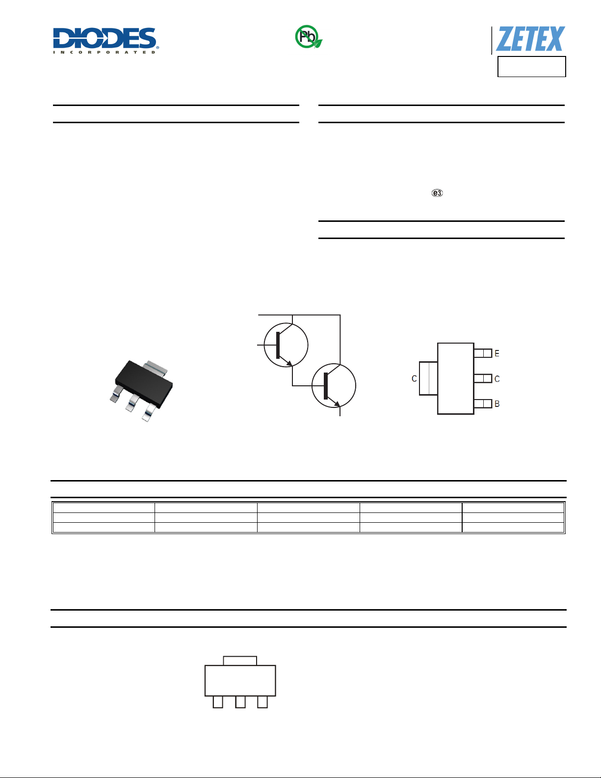
SOT223
Top View
C
B
Device S
Case: SOT223
Case material: molded plastic. “Green” molding compound.
UL Flammability Rating 94V-0
Moisture Sensitivity: Level 1 per J-STD-020
Terminals: Finish - Matte Tin Plated Leads, Solderable per
MIL-STD-202, Method 208
Weight: 0.112 grams (approximate)
Applications
Lamp
Relay
Solenoid Driving
E
mbol
Top View
Pin-Out
Ordering Information (Note 4)
Product Marking Reel size (inches) Tape width (mm) Quantity per reel
FZT605TA FZT605 7 12 1,000
FZT605TC FZT605 13 12 4,000
Notes: 1. EU Directive 2002/95/EC (RoHS) & 2011/65/EU (RoHS 2) compliant. All applicable RoHS exemptions applied.
2. See http://www.diodes.com/quality/lead_free.html for more information about Diodes Incorporated’s definitions of Halogen- and Antimony-free, "Green"
and Lead-free.
3. Halogen- and Antimony-free "Green” products are defined as those which contain <900ppm bromine, <900ppm chlorine (<1500ppm total Br + Cl) and
<1000ppm antimony compounds.
4. For packaging details, go to our website at http”//www.diodes.com/products/packages.html.
Marking Information
FZT605
Document number: DS33147 Rev. 5 - 2
FZT
FZT
7053
FZT605= Product Type Marking Code
1 of 7
www.diodes.com
© Diodes Incorporated
April 2013

A
f
Maximum Ratings (@T
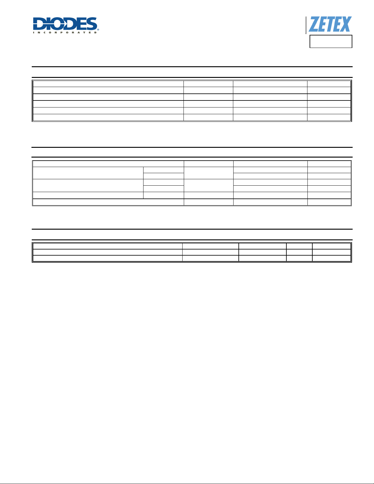
Collector-Base Voltage
Collector-Emitter Voltage
Emitter-Base Voltage
Continuous Collector Current
Peak Pulse Current
Thermal Characteristics (@T
Power Dissipation
Thermal Resistance, Junction to Ambient
Thermal Resistance, Junction to Leads (Note 7)
Operating and Storage Temperature Range
= +25°C, unless otherwise specified.)
A
Characteristic Symbol Value Unit
= +25°C, unless otherwise specified.)
A
Characteristic Symbol Value Unit
(Note 5)
(Note 6) 3 W
(Note 5)
(Note 6) 41.7
ESD Ratings (Note 8)
V
CBO
V
CEO
V
EBO
I
I
CM
P
R
θJA
R
T
J, TSTG
C
θJL
Product Line o
Diodes Incorporated
FZT605
D
140 V
120 V
14 V
1.5 A
4 A
2 W
62.5
12.93
-55 to +150
C/W
C/W
C/W
C
Electrostatic Discharge - Human Body Model ESD HBM 4,000 V 3A
Electrostatic Discharge - Machine Model ESD MM ≥ 400 V C
Notes: 5. For a device mounted on 25mm X 25mm 1oz weight copper that is on a single-sided FR4 PCB; device is measured under still air conditions whilst
operating in a steady-state.
6. Same as note (5), except the device is mounted on 50mm X 50mm 2oz copper.
7. Thermal resistance from junction to solder-point (at the end of the collector lead).
8. Refer to JEDEC specification JESD22-A114 and JESD22-A115.
Characteristic Symbol Value Unit JEDEC Class
FZT605
Document number: DS33147 Rev. 5 - 2
2 of 7
www.diodes.com
April 2013
© Diodes Incorporated

A
f
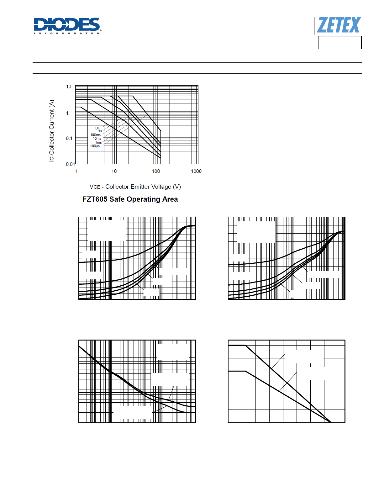
Thermal Characteristics and Derating Information
Product Line o
Diodes Incorporated
FZT605
70
T
=25°C
60
50
40
amb
25mm x 25mm
2oz FR4
D=0.5
30
D=0.2
20
10
0
100µ 1m 10m 100m 1 10 100 1k
Thermal Resistance (°C/W)
Pulse Width (s)
Single Pulse
D=0.05
D=0.1
Transient Thermal Impedance
Single Pulse
T
100
10
=25°C
amb
50mm x 50mm
2oz FR4
50
T
=25°C
40
amb
50mm x 50mm
2oz FR4
30
D=0.5
20
D=0.2
10
0
100µ 1m 10m 100m 1 10 100 1k
Thermal Resistance (°C/W)
Pulse Width (s)
Single Pulse
D=0.05
D=0.1
Transient Thermal Impedance
3.0
2.5
2.0
1.5
1.0
50mm x 50mm
2oz FR4
25mm x 25mm
2oz FR4
25mm x 25mm
2oz FR4
1
100µ 1m 10m 100m 1 10 100 1k
Max Power Dissipation (W)
Pulse Width (s)
Pulse Power Dissipation
FZT605
Document number: DS33147 Rev. 5 - 2
3 of 7
www.diodes.com
0.5
0.0
0 20 40 60 80 100 120 140 160
Max Power Dissipation (W)
Temperature (°C)
Derating Curve
April 2013
© Diodes Incorporated
 Loading...