

Page 1
A
f
Features and Benefits
• BV
• I
• I
• Low Saturation Voltage V
• h
• 500mW power dissipation
• Complementary part number FMMTL618
• Lead Free, RoHS Compliant (Note 1)
• Halogen and Antimony Free "Green" Device (Note 2)
• Qualified to AEC-Q101 Standards for High Reliability
> -20V
CEO
= -1A Continuous Collector Current
C
= -2A Peak Pulse Current
CM
< -320mV @ -1A
characterised up to -1.5A for high current gain hold-up
FE
CE(sat)
SOT23
Product Line o
Diodes Incorporated
FMMTL718
20V PNP SILICON LOW SATURATION TRANSISTOR IN SOT23
Mechanical Data
• Case: SOT-23
• UL Flammability Rating 94V-0
• Case material: molded Plastic.
• Moisture Sensitivity: Level 1 per J-STD-020D
• Terminals: Matte Tin Finish annealed over Copper plated Alloy
42 leadframe. Solderable per MIL-STD-202, Method 208
• Weight: 0.008 grams (Approximate)
Applications
• MOSFET Gate Driving
• DC-DC Converters
• Charging circuit
• Power switches
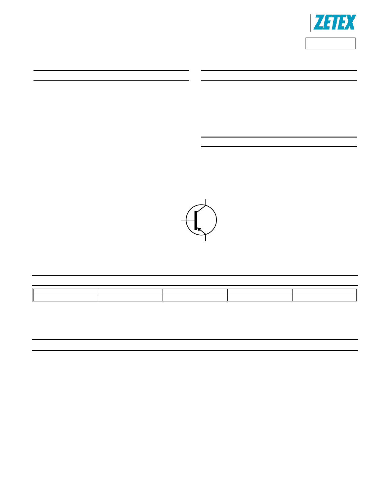
C
B
Top View
E
Device Symbol
Top View
-
Ordering Information (Note 3)
Product Marking Reel size (inches) Tape width (mm) Quantity per reel
FMMTL718TA L78 7 8 3,000
Notes: 1. No purposefully added lead.
2. Diodes Inc.`s “Green” Policy can be found on our website at http://www.diodes.com
3. For Packaging Details, go to our website at http://www.diodes.com.
Marking Information
FMMTL718
Document Number: DS33132 Rev. 2 - 2
L78 = Product Type Marking Code
1 of 5
www.diodes.com
June 2011
© Diodes Incorporated
Page 2
A
f
)
)
)
Product Line o
Diodes Incorporated
FMMTL718
Maximum Ratings @T
= 25°C unless otherwise specified
A
Characteristic Symbol Value Unit
Collector-Base Voltage
Collector-Emitter Voltage
Emitter-Base Voltage
Continuous Collector Current
Peak Pulse Current
Base Current
V
CBO
V
CEO
V
EBO
I
C
I
CM
I
B
-20 V
-20 V
-5 V
-1 A
-2 A
-200 mA
Thermal Characteristics @T
= 25°C unless otherwise specified
A
Characteristic Symbol Value Unit
Power Dissipation (Note 4) PD 500 mW
Thermal Resistance, Junction to Ambient (Note 4)
Thermal Resistance, Junction to Lead (Note 5)
Operating and Storage Temperature Range T
Notes: 4. For a device surface mounted on 15mm X 15mm FR4 PCB with high coverage of single sided 1 oz copper, in still air conditions; the device is measured
Electrical Characteristics @T
when operating in a steady-state condition.
5. Thermal resistance from junction to solder-point (at the end of the collector lead).
= 25°C unless otherwise specified
A
R
θJA
R
θJL
-55 to +150
J, TSTG
250
197
°C/W
°C/W
°C
Characteristic Symbol Min Typ Max Unit Test Condition
Collector-Base Breakdown Voltage
Collector-Emitter Breakdown Voltage (Note 6)
Emitter-Base Breakdown Voltage
Collector Cutoff Current
Emitter Cutoff Current
Collector Emitter Cutoff Current
Static Forward Current Transfer Ratio
(Note 6)
Collector-Emitter Saturation Voltage
(Note 6)
Base-Emitter Turn-On Voltage(Note 6)
Base-Emitter Saturation Voltage(Note 6)
Equivalent On-Resistance
Output Capacitance
Transition Frequency
Turn-On Time
Turn-Off Time
Note: 6.
Measured under pulsed conditions. Pulse width ≤ 300 µs. Duty cycle ≤ 2%
BV
BV
BV
I
I
I
V
CE(sat)
V
BE(on
V
BE(sat
R
CE(sat
C
CBO
CEO
EBO
CBO
EBO
CES
h
FE
obo
f
T
t
on
t
off
-20 -65 V
-20 -55 V
-5 -8.8 V
-10 nA
-10 nA
-10 nA
300
300
200
120
50
500
450
320
200
80
-33
-130
-230
-315
-50
-180
-320
-450
-0.85 -1.0 V
-0.95 -1.1 V
210 mΩ I
9 12 pF
265 MHz
108 ns
121 ns
mV
mV
mV
mV
IC = -100 µA
IC = -10 mA
I
= -100 µA
E
V
CB
V
EB
VCE= -15V
I
= -10mA, V
C
I
= -100mA, VCE = -2V
C
I
= -0.5A, VCE = -2V
C
= -1A, VCE = -2V
I
C
I
= -1.5A, V
C
I
=- 100mA, IB = -10mA
C
I
=- 500mA, IB = -20mA
C
I
= -1A, IB = -50mA
C
= -1.5A, IB = -100mA
I
C
I
= -1.25A, V
C
I
= -1.25A, I
C
= -1.5A
C
V
CB
V
CE
f = 100MHz
V
CC
I
B1
= -15V
= -4V
= -2V
CE
= -2V
CE
= -2V
CE
= -100mA
B
= -10V, f = 1MHz
= -10V, IC = -50mA,
=-10V, IC =-1A
= IB2 = -10mA
FMMTL718
Document Number: DS33132 Rev. 2 - 2
2 of 5
www.diodes.com
June 2011
© Diodes Incorporated
Page 3

A
f
Typical Electrical Characteristics
Product Line o
Diodes Incorporated
FMMTL718
FMMTL718
Document Number: DS33132 Rev. 2 - 2
3 of 5
www.diodes.com
June 2011
© Diodes Incorporated
Page 4

A
f
Product Line o
Diodes Incorporated
FMMTL718
Package Outline Dimensions
K
J
A
C
B
H
K1
F
D
G
L
M
Dim Min Max Typ
A 0.37 0.51 0.40
B 1.20 1.40 1.30
C 2.30 2.50 2.40
D 0.89 1.03 0.915
F 0.45 0.60 0.535
G 1.78 2.05 1.83
H 2.80 3.00 2.90
J 0.013 0.10 0.05
K 0.903 1.10 1.00
K1 - - 0.400
L 0.45 0.61 0.55
M 0.085 0.18 0.11
α
SOT23
0° 8° -
All Dimensions in mm
Suggested Pad Layout
Y
Z
X
E
FMMTL718
Document Number: DS33132 Rev. 2 - 2
www.diodes.com
Dimensions Value (in mm)
C
4 of 5
Z 2.9
X 0.8
Y 0.9
C
E
2.0
1.35
June 2011
© Diodes Incorporated
Page 5

A
f
Product Line o
IMPORTANT NOTICE
DIODES INCORPORATED MAKES NO WARRANTY OF ANY KIND, EXPRESS OR IMPLIED, WITH REGARDS TO THIS DOCUMENT,
INCLUDING, BUT NOT LIMITED TO, THE IMPLIED WARRANTIES OF MERCHANTABILITY AND FITNESS FOR A PARTICULAR
PURPOSE (AND THEIR EQUIVALENTS UNDER THE LAWS OF ANY JURISDICTION).
Diodes Incorporated and its subsidiaries reserve the right to make modifications, enhancements, improvements, corrections or other
changes without further notice to this document and any product described herein. Diodes Incorporat ed does not assume an y liabi lity arising
out of the application or use of this document or any product described herein; neither does Diodes Incorporated convey any license under
its patent or trademark rights, nor the rights of others. Any Customer or user of this document or products described herein in such
applications shall assume all risks of such use and will agree to hold Diodes Incorporated and all the companies whose products are
represented on Diodes Incorporated website, harmless against all damages.
Diodes Incorporated does not warrant or accept any liability whatsoever in respect of any products purchased through unauthorized sales
channel. Should Customers purchase or use Diodes Incorporated products for any unintended or unauthorized application, Customers shall
indemnify and hold Diodes Incorporated and its representatives harmless against all claims, damages, expenses, and attorney fees arising
out of, directly or indirectly, any claim of personal injury or death associated with such unintended or unauthorized application.
Products described herein may be covered by one or more United States, international or foreign patents pending. Product names and
markings noted herein may also be covered by one or more United States, international or foreign trademarks.
LIFE SUPPORT
Diodes Incorporated products are specifically not authorized for use as critical components in life support devices or systems without the
express written approval of the Chief Executive Officer of Diodes Incorporated. As used herein:
A. Life support devices or systems are devices or systems which:
1. are intended to implant into the body, or
2. support or sustain life and whose failure to perform when properly used in accordance with instructions for use provided in
the labeling can be reasonably expected to result in significant injury to the user.
B. A critical component is any component in a life sup port devic e or s ystem whose failure to p erfo rm can be re asonabl y expected to cause
the failure of the life support device or to affect its safety or effectiveness.
Customers represent that they have all necessary expertise in the safety and regulatory ramifications of their life support devices or systems,
and acknowledge and agree that they are solely responsible for all legal, regulatory and safety-related requirements concerning their
products and any use of Diodes Incorporated products in such safety-critical, life support devices or systems, notwithstanding any devicesor systems-related information or support that may be provided by Diodes Incorporated. Further, Customers must fully indemnify Diodes
Incorporated and its representatives against any damages arising out of the use of Diodes Incorpor ated products in such safety-critical, life
support devices or systems.
Copyright © 2011, Diodes Incorporated
www.diodes.com
Diodes Incorporated
FMMTL718
FMMTL718
Document Number: DS33132 Rev. 2 - 2
5 of 5
www.diodes.com
June 2011
© Diodes Incorporated
 Loading...