

Page 1
FMMTA0 6
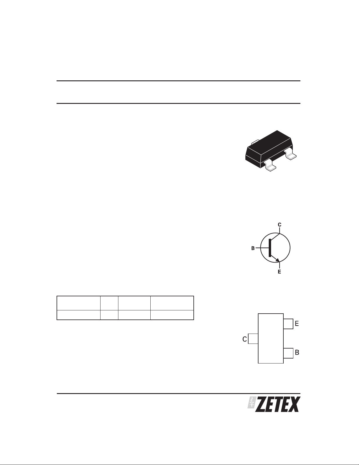
SOT23 NPN SILICON PLANARMEDIUM POWER TRA NSISTORS
SUMM ARY
V
(BR)CEO
> 80V
C(cont)
= 500mA
I
DESCRIPTION
80V mediumpower NPNtransistor in a compact SOT23
package
FEATURES
80V V
•
•
•
CEO
Compac t SOT 23 pa c k a ge
HFE50 @ IC= 100mA
APPLICATIONS
•
Low pow er mot or driv ing c irc uits
ORDERING INFORMATION
DEVICE REEL
FMMTA06TA
SIZE
7” 8mm 3,000
TAPE WIDTH
QUANTITY PER
REEL
S
T
2
3
O
SYMBOL
PINOUT
DEVICE MARKING
•
1G
ISSUE 2 - MAY 2004
TOP VIEW
1
SEMICONDUCTORS
Page 2
FMMTA0 6
ABS OLUT E MA X IMUM RA T I NGS
PAR AMETER SYMBO L LIMIT UNIT
Colle ctor-base voltage V
Colle ctor-emitter voltage V
Emitter-base voltage V
Peak pulse current I
Continuous c olle ctor current I
Base c urrent I
Pow e r dissipation @ T
= 25° C
A
P
CBO
CEO
EBO
CM
C
B
D
Linear derating factor
Operating and storage temperature T
j;Tstg
THERMAL RESIST A NCE
PAR AMETER SYMBOL VALUE UNIT
Junction t o ambient
R⍜
JA
80 V
80 V
4V
1A
500 mA
100 mA
330
2.64
mW
mW/° C
-55 to + 150 °C
379 ° C/W
SEMICONDUCTORS
ISSUE 2 - MAY 2004
2
Page 3

CHARACTERISTICS
FMMTA0 6
ISSUE 2 - MAY 2004
3
SEMICONDUCTORS
Page 4

FMMTA0 6
ELECTRICAL CHARAC TERISTICS (at T
= 25° C unles s ot herwis e s t ated)
amb
PARAMETER S YMBOL MIN. TYP. MAX. UNIT COND ITI O NS
Colle ctor-base breakdown voltage V
Colle ctor-emitter breakdown voltage V
Emitter-base breakdown voltage V
Colle ctor-emitter cut-off current I
Colle ctor-base cut-off curre nt I
St a tic forw ard c urrent transf er ratio H
Colle ctor-emitter saturation voltage V
Base-emitter turn-on voltage V
Transition f requency f
NOTES
* Me as ured under puls e d c ondit ions . Pulse width= 3 00 S. Duty cycle ⱕ2%
(BR)CBO
(BR)CEO
(BR)EBO
CES
CBO
FE
CE(sat)
BE(on)
T
80 V IC=1mA
80
4V
100 nA V
100
V
nA
IC= 10mA*
I
= 100A
E
= 60V
CES
VCB= 80V
5050120 IC= 10mA, VCE=1V*
= 100mA, VCE=1V*
I
C
0.25 V IC= 100mA, IB= 10mA*
1.2 V IC=0.1A,VCE=1V*
100 IC= 10mA, VCE=2V,
f= 100MHz
SEMICONDUCTORS
ISSUE 2 - MAY 2004
4
Page 5

TYPICAL CHARACTERISTICS
FMMTA0 6
ISSUE 2 - MAY 2004
5
SEMICONDUCTORS
Page 6

FMMTA0 6
PACKAGE OUTLINE
Controlling dimensions are in millimet ers . A pprox imat e conve rsions are give n in inc hes
PA CK AGE D I ME NSI O NS
DIM
Min Max Min Max Min Max Max Max
DIM
A 2.67 3.05 0.105 0.120 H 0.33 0.51 0.013 0.020
B 1.20 1.40 0.047 0.055 K 0.01 0.10 0.0004 0.004
Millimeters Inches
C
1.10
ᎏ
0.043 L 2.10 2.50 0.083 0.0985
ᎏ
D 0.37 0.53 0.015 0.021 M 0.45 0.64 0.018 0.025
F 0.085 0.15 0.0034 0.0059 N 0.95 NOM 0.0375 NOM
G 1.90 NOM 0.075 NOM
Millimeters Inches
ᎏᎏ ᎏ
©Z etex Semic onduc t ors plc 2004
Europe
Zetex GmbH
Streitfeldstraße 19
D-81673 München
Germany
Telefon: (49) 89 45 49 49 0
Fax: (49) 89 45 49 49 49
europe.sales@zetex.com
These of fice s a re s upport ed by age nt s and dis t ribut ors in major c ountries w orld- w ide .
This publication is issued to provide outline information only which (unless agreed by the Company in writing) may not be used, applied or reproduced for
any purpose orformpart of any order orcontract or be regarded as a representation relating to the products or services concerned. The Company reserves
the right to a lt er without notice t he s pec ifica t ion, design, price or c ondit ions of supply of any produc t or service.
For the latest product information, log on to www.zetex.com
Americas
Zetex Inc
700 Veterans Memorial Hwy
Hauppauge, NY 11788
USA
Telephone: (1) 631 360 2222
Fax: (1) 631 360 8222
usa.sales@zetex.com
Asia P ac ific
Zetex (Asia) Ltd
3701-04 Metroplaza Towe r 1
Hing F ong R oad, Kw ai Fong
Hong Kong
Telephone: (852) 26100 611
Fax: (852) 24250 494
asia.sales@zetex.com
Corporate He adquat ers
Zet ex Semiconductors plc
Zet ex T echnology Park, Chadde rt on
Oldham, OL9 9 LL
United Kingdom
Telephone ( 44 ) 16 1 622 4444
Fax: (44) 161 622 4446
hq@zetex.com
ISSUE 2 - MAY 2004
SEMICONDUCTORS
6
 Loading...