Diodes DZT5551 User Manual

Features
• BV
• BV
• I
• Low Saturation Voltage (150mV max @10mA)
• h
• Complementary PNP Type: DZT5401
• Totally Lead-Free & Fully RoHS Compliant (Notes 1 & 2)
• Halogen and Antimony Free. “Green” Device (Note 3)
• Qualified to AEC-Q101 Standards for High Reliability
> 160V
CEO
> 6V
EBO
= 600mA Continuous Collector Current
C
specified up to 50mA for a high gain hold up
FE
Applications
• High Voltage Amplification Applications
• High Voltage Switching
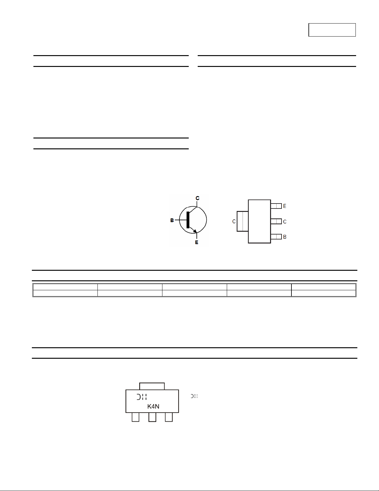
SOT223
Top View
Mechanical Data
• Case: SOT223
• Case material: molded plastic. “Green” molding compound.
• UL Flammability Rating 94V-0
• Moisture Sensitivity: Level 1 per J-STD-020
• Terminals: Finish - Matte Tin Plated Leads, Solderable per
• Weight: 0.112 grams (approximate)
Device Schematic
DZT5551
160V NPN VOLTAGE TRANSISTOR IN SOT223
MIL-STD-202, Method 208
Pin-Out Top View
Ordering Information (Note 4)
Part Number Marking Reel size (inches) Tape width (mm) Quantity per reel
DZT5551-13 K4N 13 12 2,500
Notes: 1. No purposely added lead. Fully EU Directive 2002/95/EC (RoHS) & 2011/65/EU (RoHS 2) compliant.
3. Halogen and Antimony free "Green” products are defined as those which contain <900ppm bromine, <900ppm chlorine (<1500ppm total Br + Cl) and
4. For packaging details, go to our website at http://www.diodes.com
2. See http://www.diodes.com for more information about Diodes Incorporated’s definitions of Halogen and Antimony free,"Green" and Lead-Free.
<1000ppm antimony compounds.
Marking Information
DZT5551
Document number: DS31219 Rev. 3 - 2
(Top View)
K4N = Product type marking code
Y
W
W
www.diodes.com
= Manufacturer’s code marking
YWW = Date code marking
Y = Last digit of year ex: 7 = 2007
WW = Week code 01 - 52
1 of 7
November 2012
© Diodes Incorporated

θ
θ
Maximum Ratings (@T
= +25°C, unless otherwise specified.)
A
Characteristic Symbol Value Unit
Collector-Base Voltage
Collector-Emitter Voltage
Emitter-Base Voltage
Continuous Collector Current
Peak Collector Current
V
CBO
V
CEO
V
EBO
I
C
I
CM
180 V
160 V
6 V
600 mA
1 A
Thermal Characteristics
Characteristic Symbol Value Unit
Power Dissipation (Note 5)
Thermal Resistance, Junction to Ambient (Note 5)
Thermal Resistance, Junction to Leads (Note 6)
Operating and Storage Temperature Range
Notes: 5. Device mounted on 50mm X 50mm X 1.6mm FR-4 PCB with high coverage of single sided 1 oz. copper, in still air condition
6. Thermal resistance from junction to solder-point (at the end of the collector lead).
P
D
R
JA
R
JL
, T
T
J
STG
2 W
62.5 °C/W
34.05 °C/W
-55 to +150 °C
DZT5551
DZT5551
Document number: DS31219 Rev. 3 - 2
2 of 7
www.diodes.com
November 2012
© Diodes Incorporated

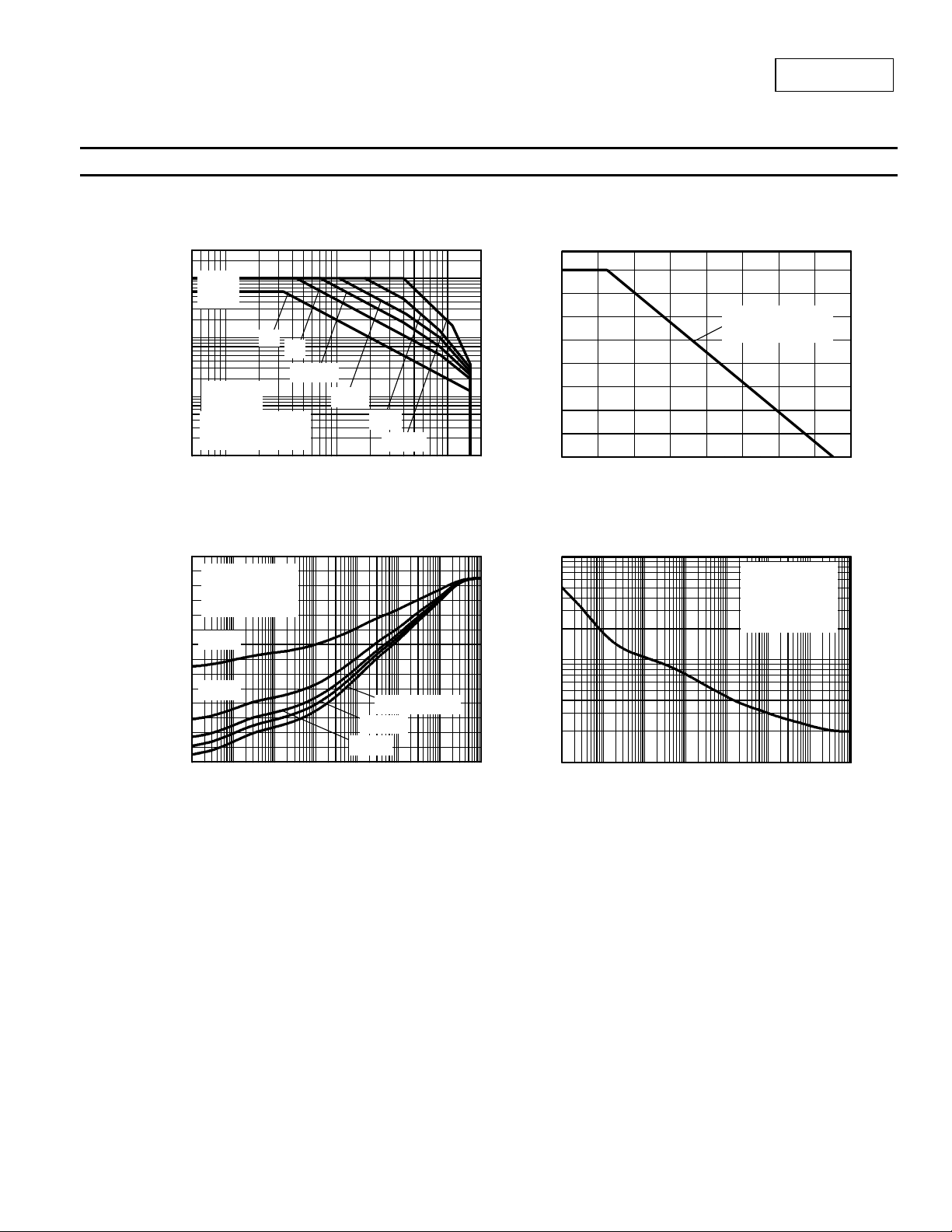
Thermal Characteristics and Derating Information
DZT5551
1
V
CE(sat)
Limited
100m
10m
Collect o r Cu rr e nt (A)
C
I
Single Pulse
T
50mmx50mmx1.6mm
1oz Copper
1m
DC
1s
100ms
amb
=25°C
10ms
1ms
100µs
1 10 100
VCE Collector-Emitter Voltage (V)
Safe Operating Area
70
T
=25°C
60
50
40
30
20
10
100µ 1m 10m 100m 1 10 100 1k
Thermal Resistance (° C /W)
amb
50mmx50mmx1.6mm
1oz Copper
D=0.5
D=0.2
Single Pulse
D=0.05
D=0.1
0
Pulse Width (s)
2.00
1.75
1.50
1.25
50mmx50mmx1.6mm
1oz Copper
1.00
0.75
0.50
0.25
0.00
0 20 40 60 80 100 120 140 160
Max Power Dissipation (W)
Temperature (°C)
Dera ting C urv e
100
10
Maximum Power (W)
1
100µ 1m 10m 100m 1 10 100 1k
Pulse Width (s)
Single Pulse
T
=25°C
amb
50mmx50mmx1.6mm
1oz Copper
Transient Thermal Impedance
DZT5551
Document number: DS31219 Rev. 3 - 2
3 of 7
www.diodes.com
Pulse Power Dissipation
November 2012
© Diodes Incorporated
 Loading...