

Diodes DZT5401 User Manual
R
Features
• Epitaxial Planar Die Construction
• Complementar
• Ideally
y NPN Type Available (DZT5551)
Suited for Automated Assembly Processes
• Ideal for Medium
• Lead Free
• "Gree
By Design/RoHS Compliant (Note 1)
n" Device (Note 3)
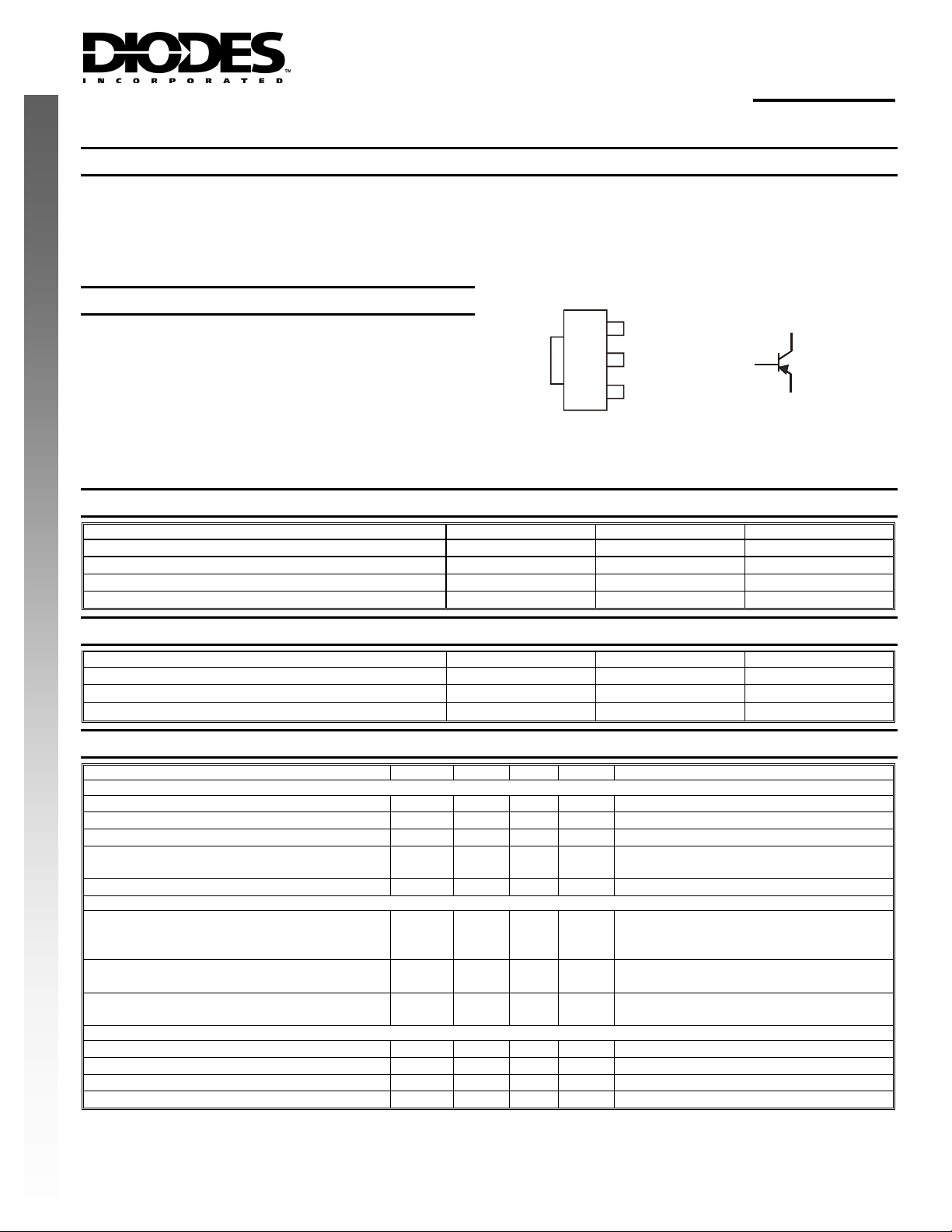
Mechanical Data
• Case: SOT-223
• Case Material:
UL Flammability Classification Rating 94V-0
• Moisture Sensitivity
• Terminals: Finish - Matte Tin a
NEW PRODUCT
(Lead Free Plating). Solderable per MIL-STD-202, Method 208
• Terminal Conn
• Marking & T
• Orde
ring Information: See Page 3
ections: See Diagram
ype Code Information: See Page 3
• Weight: 0.112 gr
Power Switching or Amplification Applications
Molded Plastic, "Green" Molding Compound.
: Level 1 per J-STD-020C
nnealed over Copper Leadframe
ams (approximate)
C
4
TOP VIEW
DZT5401
PNP SURFACE MOUNT TRANSISTOR
3
2
1
4
SOT-223
3
E
C
2
B
1
Schematic and Pin Configuration
COLLECTOR
1
BASE
2,4
3
EMITTE
Maximum Ratings @T
= 25°C unless otherwise specified
A
Characteristic Symbol Value Unit
Collector-Base Voltage
Collector-Emitter Voltage
Emitter-Base Voltage
Collector Current
V
CBO
V
CEO
V
EBO
I
C
-160 V
-150 V
-5.0 V
-600 mA
Thermal Characteristics
Characteristic Symbol Value Unit
Power Dissipation @TA = 25°C (Note 3) P
Thermal Resistance, Junction to Ambient @TA = 25°C (Note 3)
Operating and Storage Temperature Range
Electrical Characteristics @T
OFF CHARACTERISTICS (Note 4)
Collector-Base Breakdown Voltage
Collector-Emitter Breakdown Voltage
Emitter-Base Breakdown Voltage
Collector Cutoff Current
Emitter Cutoff Current
ON CHARACTERISTICS (Note 4)
DC Current Gain
Collector-Emitter Saturation Voltage
Base-Emitter Saturation Voltage
SMALL SIGNAL CHARACTERISTICS
Output Capacitance
Small Signal Current Gain
Current Gain-Bandwidth Product
Noise Figure NF
Notes: 1. No purposefully added lead.
2. Diodes Inc.'s "Green" policy can be found on our website at http://www.diodes.com/products/lead_free/index.php.
3. Device mounted on FR-4 PCB, pad layout as shown on page 4
website at http://www.diodes.com/data
4. Measured under pulsed conditions. Pulse width = 300ms. Duty cycle ≤ 2
DS31218 Rev. 2 – 2
Characteristic Symbol Min Max Unit Test Condition
= 25°C unless otherwise specified
A
V
(BR)CBO
V
(BR)CEO
V
(BR)EBO
I
CBO
I
EBO
-160
-150
-5.0
⎯
⎯
50
h
V
CE(SAT)
V
BE(SAT)
C
h
f
FE
obo
fe
T
60
50
⎯
⎯
⎯
40 200
100 300 MHz
⎯
sheets/ap02001.pdf.
or in Diodes Inc. suggested pad layout document AP02001, which can be found on our
www.diodes.com
D
R
JA
θ
T
, T
j
STG
240
-0.2
-0.5
-1.0 V
%.
1 of 4
⎯
⎯
⎯
-50
-50 nA
⎯
⎯
V
I
V
I
V
I
nA
V
μA
V
V
I
I
⎯
I
I
V
I
I
I
6.0 pF
VCB = -10V, f = 1.0MHz, IE = 0
⎯ V
V
8.0 dB
V
125
-55 to +150
= -100μA, IE = 0
C
= -1.0mA, IB = 0
C
= -10μA, IC = 0
E
= -120V, IE = 0
CB
= -120V, IE = 0, TA = 150°C
CB
= -3.0V, IC = 0
EB
= -1.0mA, VCE = -5.0V
C
= -10mA, VCE = -5.0V
C
= -50mA, V
C
= -10mA, IB = -1.0mA
C
= -50mA, IB = -5.0mA
C
= -10mA, IB = -1.0mA
C
= -50mA, IB = -5.0mA
C
= -10V, IC = -1.0mA, f = 1.0kHz
CE
= -10V, IC = -10mA, f = 100MHz
CE
= -5.0V, IC = -200μA, RS = 10Ω, f = 1.0kHz
CE
1 W
°C/W
°C
= -5.0V
CE
DZT5401
© Diodes Incorporated
P, P
OWER
P
TIO
C
O
CTO
R
C
U
R
REN
T
C
O
CTO
R
T
TER
MIT
T
R
T
U
R
N
O
N
O
TAG
T
T
R
TURAT
O
OLT
G
1.0
0.8
(A)
0.25
0.20
I = -6mA
B
I = -8mA
B
I = -10mA
B
N (mW)
I = -4mA
A
0.6
0.15
B
I = -2mA
B
DISSI
0.4
0.10
LLE
NEW PRODUCT
D
0.2
0
0
25 50
T , AMBIENT TEMPERATURE (°C)
A
75
100 125
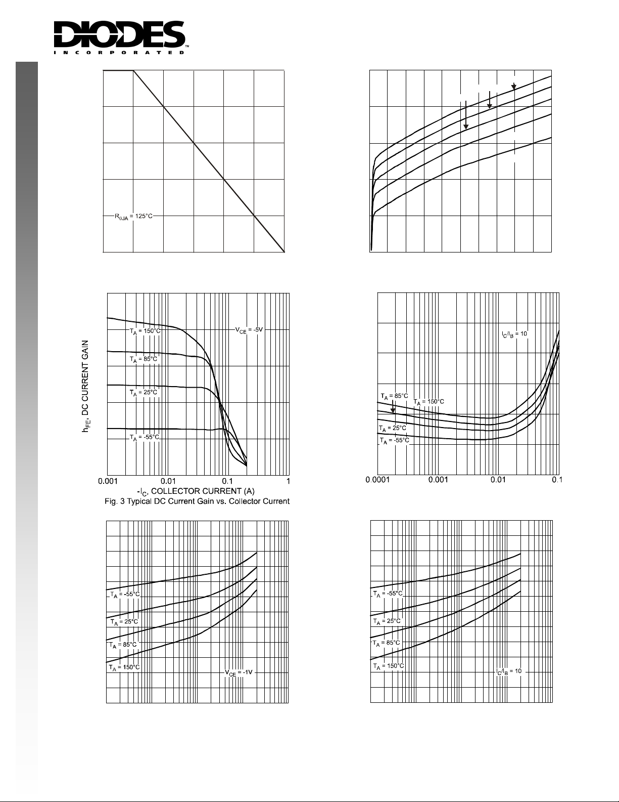
Fig. 1 Max Po wer D issipation vs. Ambient Temperature
250
200
150
100
50
0
1.2
E (V)
1
L
V
0.8
-
150
C
0.05
-I ,
0.00
012345678910
-V , COLLECTOR-EMITTER VOL TAGE (V)
Fig. 2 Typical Collector Current vs. Collector-Emitter Voltage
CE
0.3
0.25
0.2
-EMI
0.15
LLE
0.1
SATURATION VOLTAGE (V)
CE(SAT)
-V ,
0.05
0
-I , COLLECTOR CURRENT (A)
Fig. 4 Typical Collector-Emitter Saturation Voltage
C
vs. Collector Current
1.2
E (V)
A
1
N V
0.8
I
0.6
E
0.4
0.2
BE(ON)
0
-V , BASE-E
0.0001 0.001 0.01 0.1 1
-I , COLLECTOR CURRENT (A)
C
Fig. 5 Typical Base-Emitter Turn-On V o ltage
vs. Collec to r Current
0.6
SA
E
0.4
0.2
0
0.0001 0.001 0.01 0.1 1
BE(SAT)
-V , BASE-EMI
-I , COLLECTOR CURRENT (A)
C
Fig. 6 Typical Base-Emitter Saturation Voltage
vs. Collector Current
DS31218 Rev. 2 – 2
2 of 4
www.diodes.com
DZT5401
© Diodes Incorporated
 Loading...