

Page 1
Features
Dual Zeners in Common Cathode Configuration
300 mW Power Dissipation
Ideally Suited for Automated Insertion
V
Common Anode Style Available, See AZ Series
Totally Lead-Free & Fully RoHS Compliant (Notes 1 & 2)
Halogen and Antimony Free. “Green” Device (Notes 3 & 4)
Qualified to AEC-Q101 Standards for High Reliability
For Both Diodes in One Case is 5%
Z
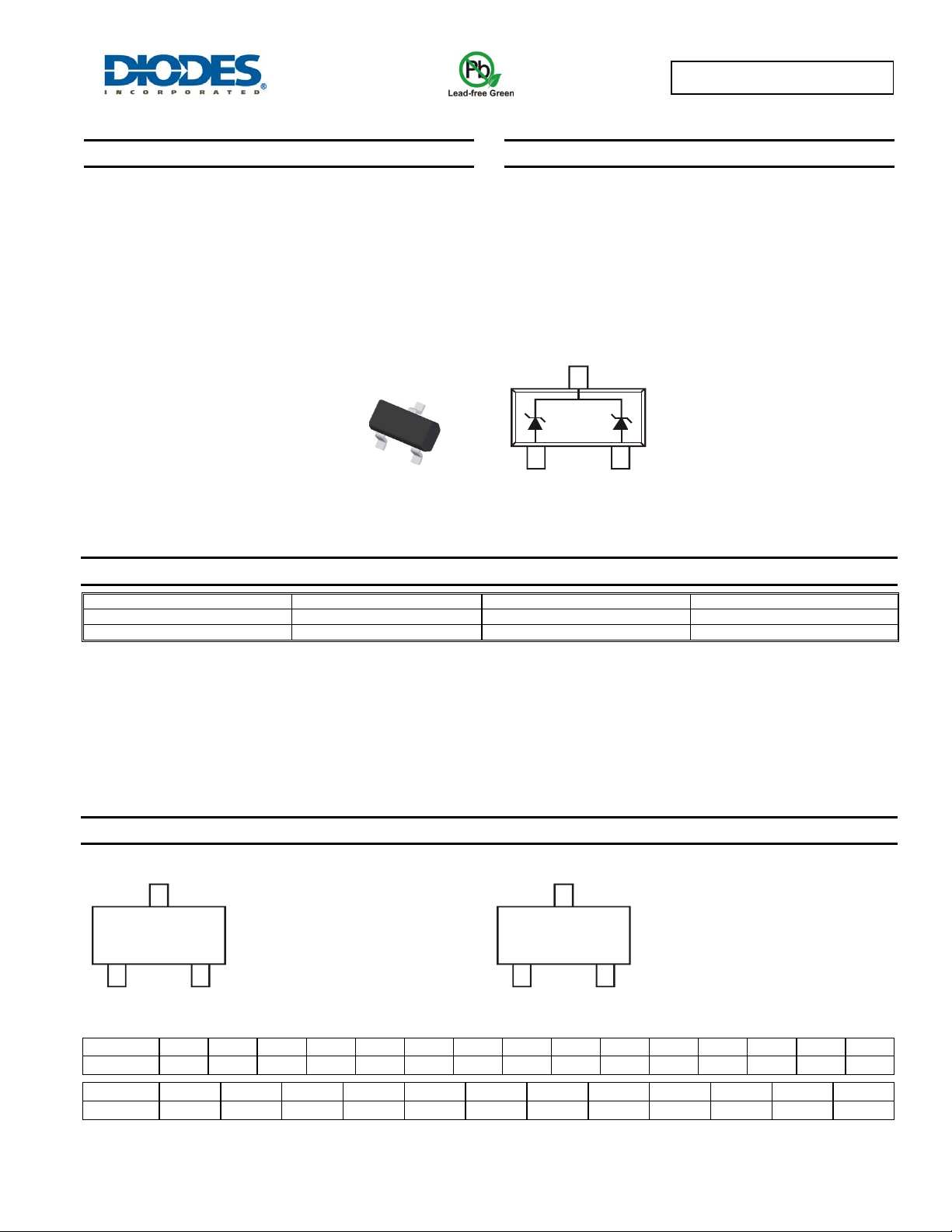
SOT23
Top View
DZ23C2V7 - DZ23C51
300mW DUAL SURFACE MOUNT ZENER DIODE
Mechanical Data
Case: SOT23
Case Material: Molded Plastic, “Green” Molding Compound. UL
Flammability Classification Rating 94V-0
Moisture Sensitivity: Level 1 per J-STD-020
Terminals: Matte Tin Finish annealed over Alloy 42 lead frame
(Lead Free Plating). Solderable per MIL-STD-202, Method 208
Polarity: See Diagram
Weight: 0.008 grams (approximate)
Device Schematic
Ordering Information (Note 5)
Device Qualification Packaging Shipping
(Type Number)-7-F* Commercial SOT23 3000/Tape & Reel
(Type Number)Q-7-F* Automotive SOT23 3000/Tape & Reel
*Add “-7-F” to the appropriate type number in Electrical Characteristics Table on Page 2. Example: 6.2V Zener = DZ23C6V2-7-F.
Notes: 1. No purposely added lead. Fully EU Directive 2002/95/EC (RoHS) & 2011/65/EU (RoHS 2) compliant.
2. See http://www.diodes.com/quality/lead_free.html for more information about Diodes Incorporated’s definitions of Halogen- and Antimony-free, "Green"
and Lead-free.
3. Halogen- and Antimony-free "Green” products are defined as those which contain <900ppm bromine, <900ppm chlorine (<1500ppm total Br + Cl) and
<1000ppm antimony compounds.
4. Product manufactured with Date Code OW (week 42, 2009) and newer are built with Green Molding Compound. Product manufactured prior to Date
Code OW are built with Non-Green Molding Compound and may contain Halogens or Sb2O3 Fire Retardants.
5. For Packaging Details, go to our website at http://www.diodes.com/products/packages.html
Marking Information
Kxx
Date Code Key
Year 1998 … 2002 2003 2004 … 2010 2011 2012 2013 2014 2015 2016 2017 2018
Code J … N P R … X Y Z A B C D E F
Month Jan Feb Mar Apr May Jun Jul Aug Sep Oct Nov Dec
Code 1 2 3 4 5 6 7 8 9 O N D
YM
DZ23C2V7 - DZ23C51
Document number: DS18002 Rev. 20 - 2
K = SAT (Shanghai Assembly / Test site)
xx = Product Type Marking Code
See Electrical Characteristics Table
YM = Date Code Marking
Y = Year (ex: Z = 2012)
M = Month (ex: 9 = September)
www.diodes.com
1 of 5
Cxx
C = CAT (Chengdu Assembly / Test site)
xx = Product Type Marking Code
See Electrical Characteristics Table
YM
YM = Date Code Marking
Y = Year (ex: Z = 2012)
M = Month (ex: 9 = September)
July 2013
© Diodes Incorporated
Page 2
K
K
DZ23C2V7 - DZ23C51
Thermal Characteristics
Characteristic Symbol Value Unit
Power Dissipation (Note 6)
Thermal Resistance, Junction to Ambient Air (Note 6)
Operating and Storage Temperature Range
Notes: 6. Mounted on FR4 PC Board with recommended pad layout which can be found on our website at http://www.diodes.com.
P
D
R
θJA
T
, T
J
STG
Electrical Characteristics (@T
Type
Number
Marking
Code
Voltage Range
@ IZT = 5.0mA ZZT @ IZT = 5.0mA Z
= +25°C, unless otherwise specified.)
A
Zener
Zener Impedance
(Note 7)
VZ (V)
Ω Ω TC (%/°C)
Maximum
f = 1kHz
Z
@ I
= 1.0mA @ IR = 0.1µA
Z
DZ23C2V7 V1 2.5-2.9 83 500 -0.065 —
DZ23C3V0 V2 2.8-3.2 95 500 -0.060 —
DZ23C3V3 V3 3.1-3.5 95 500 -0.055 —
DZ23C3V6 V4 3.4-3.8 95 500 -0.055 —
DZ23C3V9 V5 3.7-4.1 95 500 -0.050 —
DZ23C4V3 V6 4.0-4.6 95 500 -0.035 —
DZ23C4V7 V7 4.4-5.0 78 500 -0.015 —
DZ23C5V1 V8 4.8-5.4 60 480 +0.005 0.8
DZ23C5V6 V9 5.2-6.0 40 400 +0.020 1.0
DZ23C6V2 VA 5.8-6.6 10 200 +0.030 2.0
DZ23C6V8 VB 6.4-7.2 8.0 150 +0.045 3.0
DZ23C7V5 VC 7.0-7.9 7.0 50 +0.050 5.0
DZ23C8V2 VD 7.7-8.7 7.0 50 +0.055 6.0
DZ23C9V1 VE 8.5-9.6 10 50 +0.065 7.0
DZ23C10 VF 9.4-10.6 15 70 +0.065 7.5
DZ23C11 VG 10.4-11.6 20 70 +0.070 8.5
DZ23C12 VH 11.4-12.7 20 90 +0.075 9.0
DZ23C13 VI 12.4-14.1 25 110 +0.080 10.0
DZ23C15 VJ 13.8-15.6 30 110 +0.080 11.0
DZ23C16 VK 15.3-17.1 40 170 +0.090 12.0
DZ23C18 VL 16.8-19.1 50 170 +0.090 14.0
DZ23C20 VM 18.8-21.2 50 220 +0.090 15.0
DZ23C22 VN 20.8-23.3 55 220 +0.090 17.0
DZ23C24 VO 22.8-25.6 80 220 +0.090 18.0
DZ23C27 VP 25.1-28.9 80 250 +0.090 20.0
DZ23C30 VQ 28-32 80 250 +0.090 22.5
DZ23C33 VR 31-35 80 250 +0.090 25.0
DZ23C36 VS 34-38 90 250 +0.090 27.0
DZ23C39 VT 37-41 90 300 +0.110 29.0
DZ23C43 VU 40-46 100 700 +0.110 32.0
DZ23C47 VV 44-50 100 750 +0.110 35.0
DZ23C51 VW 48-54 100 750 +0.110 38.0
Notes: 7. Short duration pulse test used to minimize self-heating effect.
300 mW
417 °C/W
–65 to +150 °C
Typical
Temperature
Coefficient
Min.
Reverse
Voltage (Note 7)
VR (V)
DZ23C2V7 - DZ23C51
Document number: DS18002 Rev. 20 - 2
2 of 5
www.diodes.com
July 2013
© Diodes Incorporated
Page 3

P, P
OWER D
P
T
O
N
R CUR
R
T
R CUR
RENT
R CUR
RENT
DZ23C2V7 - DZ23C51
500
400
50
40
(mW)
I
A
300
(mA)
EN
30
ISSI
200
D
100
0
0120
30
Note 6
40 80 160
T , AMBIEMT TEMPERATURE (°C)
A
Fig. 1 Power Derating Curve
T = 25°C
j
C10
C12
200
20
Z
I, ZENE
10
0
01 234 5 6
V , ZENER VOLTAGE (V)
Fig. 2 Typical Zener Breakdown Characteristics
Z
8910
7
10
8
20
(mA)
10
Z
I, ZENE
1,000
100
C15
C18
C22
Test Current I
0
0
Z
5mA
10 20 30 40
V , ZENER VOLTAGE (V)
Z
C27
C33
Fig. 3 Typical Zener Breakdown Characteristics
C36
(mA)
6
4
Z
I, ZENE
2
0
10 20 30 40 50 60 70 80 90 100
0
V , ZENER VOLTAGE (V)
Z
Fig. 4 Typical Zener Breakdown Characteristics
T
C , TOTAL CAPACITANCE (pF)
10
1
V , NOMINAL ZENER VOLTAGE (V)
Z
10
100
Fig. 5 Typical Total Capacitance vs. Nominal Zener Voltage
DZ23C2V7 - DZ23C51
Document number: DS18002 Rev. 20 - 2
3 of 5
www.diodes.com
July 2013
© Diodes Incorporated
Page 4

Package Outline Dimensions
Please see AP02002 at http://www.diodes.com/datasheets/ap02002.pdf for latest version.
A
K
J
H
F
D
G
C
B
K1
L
M
DZ23C2V7 - DZ23C51
Dim Min Max Typ
A 0.37 0.51 0.40
B 1.20 1.40 1.30
C 2.30 2.50 2.40
D 0.89 1.03 0.915
F 0.45 0.60 0.535
G 1.78 2.05 1.83
H 2.80 3.00 2.90
J 0.013 0.10 0.05
K 0.903 1.10 1.00
K1
L 0.45 0.61 0.55
M 0.085 0.18 0.11
SOT23
0° 8°
All Dimensions in mm
0.400
Suggested Pad Layout
Please see AP02001 at http://www.diodes.com/datasheets/ap02001.pdf for the latest version.
Y
Dimensions Value (in mm)
Z
X
E
C
Z 2.9
X 0.8
Y 0.9
C
E
2.0
1.35
DZ23C2V7 - DZ23C51
Document number: DS18002 Rev. 20 - 2
4 of 5
www.diodes.com
July 2013
© Diodes Incorporated
Page 5

IMPORTANT NOTICE
DIODES INCORPORATED MAKES NO WARRANTY OF ANY KIND, EXPRESS OR IMPLIED, WITH REGARDS TO THIS DOCUMENT,
INCLUDING, BUT NOT LIMITED TO, THE IMPLIED WARRANTIES OF MERCHANTABILITY AND FITNESS FOR A PARTICULAR PURPOSE
(AND THEIR EQUIVALENTS UNDER THE LAWS OF ANY JURISDICTION).
Diodes Incorporated and its subsidiaries reserve the right to make modifications, enhancements, improvements, corrections or other changes
without further notice to this document and any product described herein. Diodes Incorporated does not assume any liability arising out of the
application or use of this document or any product described herein; neither does Diodes Incorporated convey any license under its patent or
trademark rights, nor the rights of others. Any Customer or user of this document or products described herein in such applications shall assume
all risks of such use and will agree to hold Diodes Incorporated and all the companies whose products are represented on Diodes Incorporated
website, harmless against all damages.
Diodes Incorporated does not warrant or accept any liability whatsoever in respect of any products purchased through unauthorized sales channel.
Should Customers purchase or use Diodes Incorporated products for any unintended or unauthorized application, Customers shall indemnify and
hold Diodes Incorporated and its representatives harmless against all claims, damages, expenses, and attorney fees arising out of, directly or
indirectly, any claim of personal injury or death associated with such unintended or unauthorized application.
Products described herein may be covered by one or more United States, international or foreign patents pending. Product names and markings
noted herein may also be covered by one or more United States, international or foreign trademarks.
LIFE SUPPORT
Diodes Incorporated products are specifically not authorized for use as critical components in life support devices or systems without the express
written approval of the Chief Executive Officer of Diodes Incorporated. As used herein:
A. Life support devices or systems are devices or systems which:
1. are intended to implant into the body, or
2. support or sustain life and whose failure to perform when properly used in accordance with instructions for use provided in the
labeling can be reasonably expected to result in significant injury to the user.
B. A critical component is any component in a life support device or system whose failure to perform can be reasonably expected to cause the
failure of the life support device or to affect its safety or effectiveness.
Customers represent that they have all necessary expertise in the safety and regulatory ramifications of their life support devices or systems, and
acknowledge and agree that they are solely responsible for all legal, regulatory and safety-related requirements concerning their products and any
use of Diodes Incorporated products in such safety-critical, life support devices or systems, notwithstanding any devices- or systems-related
information or support that may be provided by Diodes Incorporated. Further, Customers must fully indemnify Diodes Incorporated and its
representatives against any damages arising out of the use of Diodes Incorporated products in such safety-critical, life support devices or systems.
Copyright © 2012, Diodes Incorporated
www.diodes.com
DZ23C2V7 - DZ23C51
DZ23C2V7 - DZ23C51
Document number: DS18002 Rev. 20 - 2
5 of 5
www.diodes.com
July 2013
© Diodes Incorporated
 Loading...