Diodes DXTP03200BP5 User Manual

A
f
Features
• 43% smaller than SOT223; 60% smaller than TO252
• Maximum height just 1.1mm
• Rated up to 3.2W
• V
• I
• Low Saturation voltage
• Lead, Halogen, and Antimony Free/RoHS Compliant (Note 1)
• “Green” Device (Note 2)
= -200V
CEO
= -2A; ICM = -5A
C
Application
• DC – DC conversion
ADVANCE INFORMATION
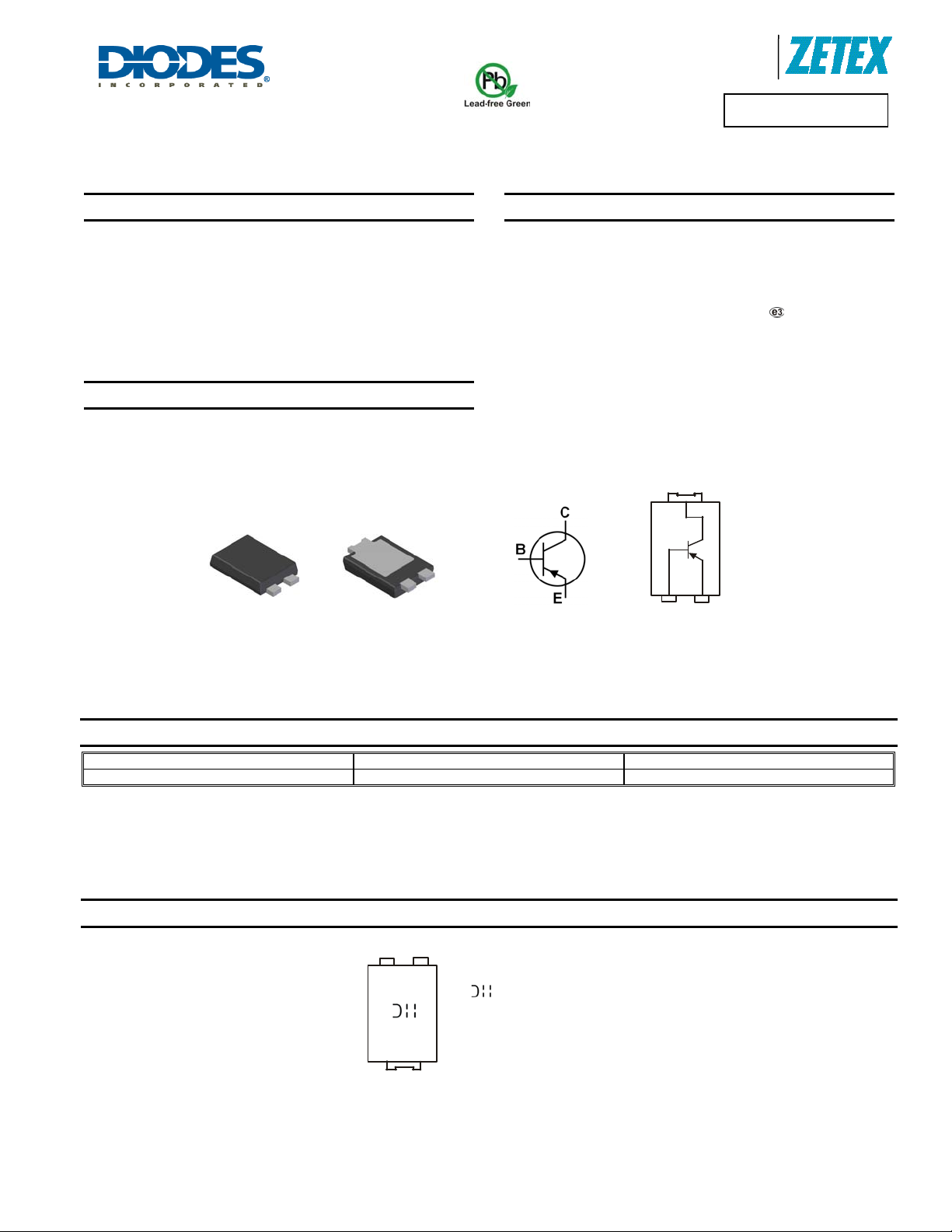
Top View Bottom View Pin-out diagram
Product Line o
Diodes Incorporated
DXTP03200BP5
200V PNP HIGH VOLTAGE TRANSISTOR
PowerDI
Mechanical Data
• Case: PowerDI®5
• Case Material: Molded Plastic, “Green” Molding Compound.
UL Flammability Classification Rating 94V-0
• Moisture Sensitivity: Level 1 per J-STD-020
• Terminals: Finish – Matte Tin annealed over Copper leadframe.
Solderable per MIL-STD-202, Method 208
• Weight: 0.093 grams (approximate)
C
BE
Device Schematic
®
5
Ordering Information (Note 3)
Part Number Case Packaging
DXTP03200BP5-13 PowerDI®5 5000/Tape & Reel
Notes: 1. No purposefully added lead. Halogen and Antimony Free.
2. Diodes Inc’s “Green” Policy can be found on our website at http://www.diodes.com
3. For packaging details, go to our website at http://www.diodes.com/datasheets/ap02007.pdf.
Marking Information
PowerDI is a registered trademark of Diodes Incorporated.
DTP3200B
YYWWK
DXTP03200BP5
Document number: DS32068 Rev. 2 - 2
DTP3200B = Product Type Marking Code
= Manufacturers’ Code Marking
K = Factory Designator
YYWW = Date Code Marking
YY = Last Two Digits of Year (ex: 09 for 2009)
WW = Week code (01 to 53)
1 of 7
www.diodes.com
March 2010
© Diodes Incorporated

A
f
θ
θ
θ
θ
Product Line o
Diodes Incorporated
DXTP03200BP5
Maximum Ratings @T
= 25°C unless otherwise specified
A
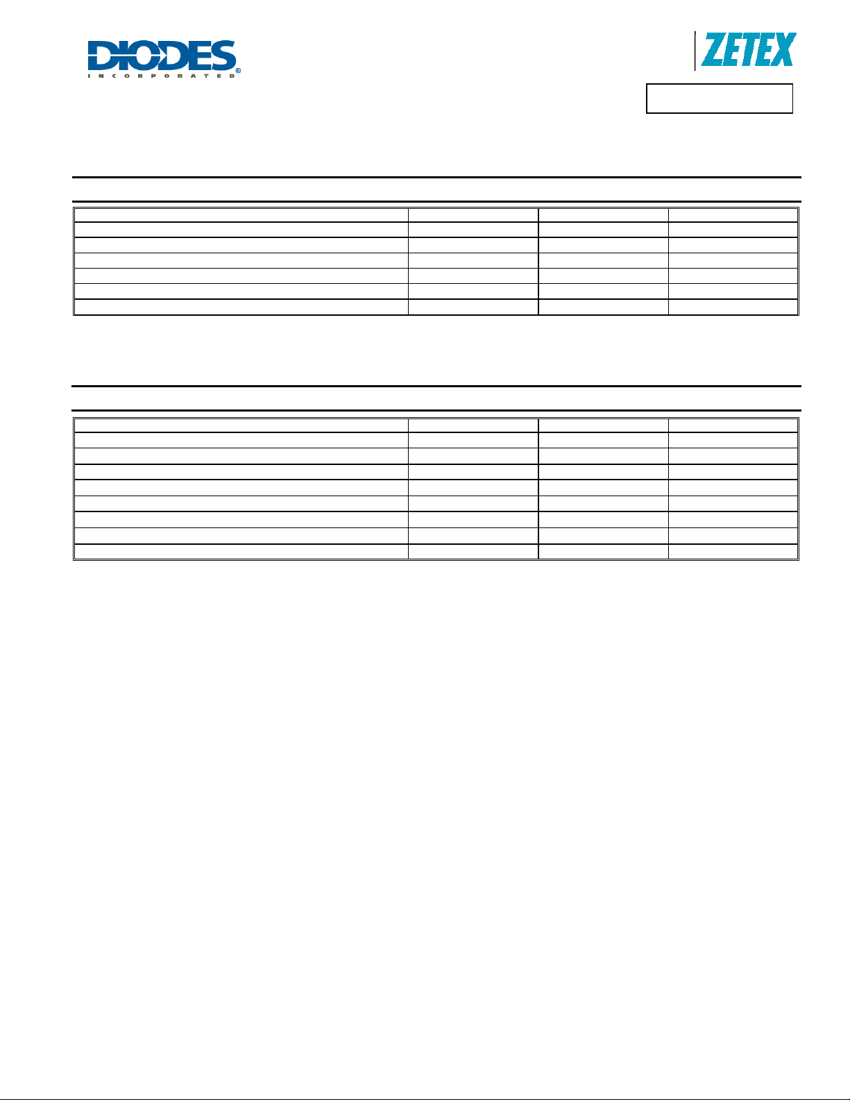
Characteristic Symbol Value Unit
Collector-Base Voltage
Collector-Emitter Voltage
Emitter-Base Voltage
Continuous Collector Current
Base Current
Peak Pulse Current
V
CBO
V
CEO
V
EBO
I
C
I
B
I
CM
-220 V
-200 V
-7 V
-2 A
-1 A
-5 A
Thermal Characteristics
Characteristic Symbol Value Unit
Power Dissipation @ TA = 25°C (Note 4) PD
Thermal Resistance, Junction to Ambient Air (Note 4) @TA = 25°C
Power Dissipation @ TA = 25°C (Note 5) PD
ADVANCE INFORMATION
Thermal Resistance, Junction to Ambient Air (Note 5) @TA = 25°C
R
JA
R
JA
Power Dissipation @ TA = 25°C (Note 6) PD
Thermal Resistance, Junction to Ambient Air (Note 6) @TA = 25°C
Thermal Resistance, Junction to Collector Terminal
Operating and Storage Temperature Range
Notes: 4. Device mounted on FR-4 PCB, single sided 2 o z. coppe r, collector pad dimensions 25mm x 25mm.
5. Device mounted on FR-4 PCB, single sided 1 oz. copper, collector pad dimensions 25mm x 25mm.
6. Device mounted on FR-4 PCB, single sided 1 oz. copper, minimum recommended pad layout.
R
JA
R
JT
, T
T
J
STG
PowerDI is a registered trademark of Diodes Incorporated.
DXTP03200BP5
Document number: DS32068 Rev. 2 - 2
2 of 7
www.diodes.com
3.2 W
39 °C/W
1.7 W
75 °C/W
0.74 W
169 °C/W
5.6 °C/W
-55 to +150 °C
March 2010
© Diodes Incorporated

A
f
Product Line o
Diodes Incorporated
DXTP03200BP5
10
V
CE(sat)
Limited
1
DC
1s
100m
Collector Cu rre nt (A)
-I
Single Pulse. T
C
10m
100m 1 10 100
100ms
See note 3
amb
10ms
=25°C
1ms
100µs
-VCE Collector-Emitter Voltage (V)
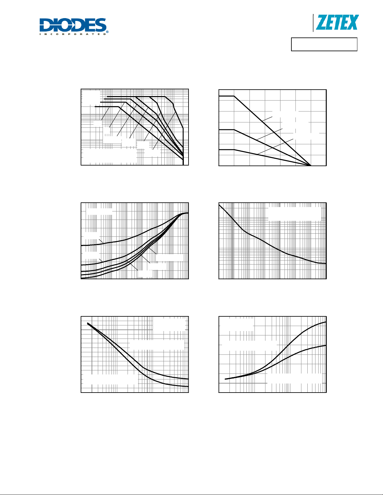
Safe Operating Area
40
ADVANCE INFORMATION
Thermal Resistance (°C/W)
See note 3
30
D=0.5
20
D=0.2
10
0
100µ 1m 10m 100m 1 10 100 1k
Single Pulse
D=0.05
D=0.1
Pulse Width (s)
Transient Thermal Impedance
3.5
3.0
2.5
2.0
1.5
1.0
0.5
0.0
0 25 50 75 100 125 150 175
Max Power Dissipation (W)
Temperature (°C)
See note 3
See note 4
See note 5
Derating Curve
Single Pulse. T
100
10
1
100µ 1m 10m 100m 1 10 100 1k
Max Power Dissipation (W)
Pulse Width (s)
amb
See note 3
Pulse Power Dissipation
=25°C
180
160
140
120
100
80
60
2 oz. weight Copper
40
20
10 100 1000 10000
Thermal Resistance (°C/W)
1 oz. weight Copper
T
=25°C
(amb)
Copper Area (sq mm)
Thermal Resistance vs. Cu Area
PowerDI is a registered trademark of Diodes Incorporated.
DXTP03200BP5
Document number: DS32068 Rev. 2 - 2
3 of 7
www.diodes.com
4
T
=25°C
(amb)
3
2 oz. weight Copper
2
1
Power Rating (W)
0
10 100 1000 10000
1 oz. weight Copper
Copper Area (sq mm)
Power Rating vs. Cu Area
March 2010
© Diodes Incorporated
 Loading...