

Page 1
θ
(BR)
(BR)
(BR)
)
)
Please click here to visit our online spice models database.
Features
• Epitaxial Planar Die Construction
• Complementary PNP Type Available (DXTA92)
• Ideally Suited for Automated Assembly Processes
• Ideal for Medium Power Switching or Amplification Applications
• Lead Free By Design/RoHS Compliant (Note 1)
• "Green" Device (Note 2)
Maximum Ratings @T
Characteristic Symbol Value Unit
Collector-Base Voltage
Collector-Emitter Voltage
Emitter-Base Voltage
Continuous Collector Current
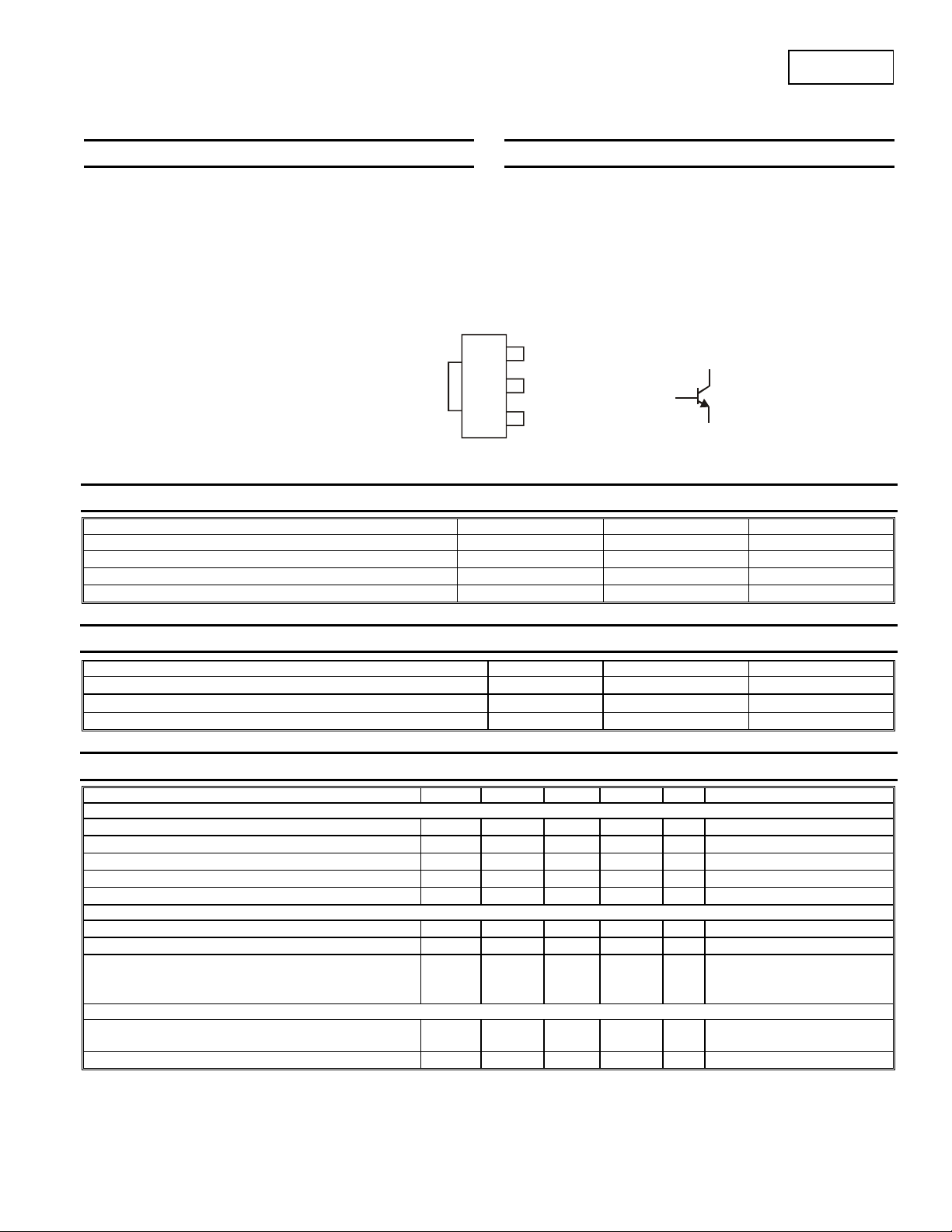
Top View
= 25°C unless otherwise specified
A
C
Device Schematic
DXTA42
NPN SURFACE MOUNT TRANSISTOR
Mechanical Data
• Case: SOT89-3L
• Case Material: Molded Plastic, "Green” Molding Compound.
UL Flammability Classification Rating 94V-0
• Moisture Sensitivity: Level 1 per J-STD-020C
• Terminals: Finish — Matte Tin annealed over Copper leadframe
(Lead Free Plating). Solderable per MIL-STD-202, Method 208
• Marking & Type Code Information: See Page 3
• Ordering Information: See Page 3
• Weight: 54.8mg (approximate)
C
3
E
2
4
O
P
T
C
1
B
W
E
I
V
V
CBO
V
CEO
V
EBO
I
C
1
S
A
B
Pin Out Configuration
300 V
300 V
6 V
500 mA
T
O
R
L
L
C
E
O
2,4
E
3
E
T
I
M
T
E
R
Thermal Characteristics
Characteristic Symbol Value Unit
Power Dissipation (Note 3) @ TA = 25°C PD
Thermal Resistance, Junction to Ambient (Note 3)
Operating and Storage Temperature Range
Electrical Characteristics @T
OFF CHARACTERISTICS (Note 4)
Collector-Base Breakdown Voltage
Collector-Emitter Breakdown Voltage
Emitter-Base Breakdown Voltage
Collector Cut-off Current
Emitter Cut-off Current
ON CHARACTERISTICS (Note 4)
Collector-Emitter Saturation Voltage
Base-Emitter Saturation Voltage
Static Forward Current Transfer Ratio
SMALL SIGNAL CHARACTERISTICS
Transition Frequency
Output Capacitance
Notes: 1. No purposefully added lead.
4. Measured under pulsed conditions. Pulse width = 300μs. Duty cycle ≤ 2%.
2. Diodes Inc.'s "Green" policy can be found on our website at http://www.diodes.com/products/lead_free/index.php.
3. Device mounted on FR-4 PCB; pad layout as shown on page 4 or in Diodes Inc. suggested pad layout document AP02001, which can
be found on our website at http://www.diodes.com/datasheets/ap02001.pdf.
DXTA42
Document number: DS31158 Rev. 4 - 2
Characteristic Symbol Min Typ Max Unit Test Conditions
= 25°C unless otherwise specified
A
V
V
V
I
I
V
CE(SAT
V
BE(SAT
CBO
CEO
EBO
CBO
EBO
300
300
⎯ ⎯
⎯ ⎯
⎯ ⎯
⎯ ⎯
25
h
FE
f
T
C
obo
40
40
50
⎯ ⎯
1 of 4
www.diodes.com
1 W
R
JA
, T
T
J
STG
⎯ ⎯
⎯ ⎯
6
⎯ ⎯
⎯ ⎯ ⎯
⎯ ⎯
125 °C/W
-55 to +150 °C
V
I
= 100μA, IE = 0
C
V
I
= 1mA, IB = 0
C
V
I
= 100μA, IC = 0
0.1
0.1
0.5 V
0.9 V
3 pF
E
μA
μA
= 200V, IE = 0
V
CB
= 6V, IC = 0
V
EB
IC = 20mA, IB = 2mA
IC = 20mA, IB = 2mA
= 1mA, VCE = 10V
I
C
I
= 10mA, VCE = 10V
C
= 30mA, VCE = 10V
I
C
= 10mA, VCE = 20V,
I
C
MHz
f = 100MHz
VCB = 20V, f = 1MHz
December 2009
© Diodes Incorporated
Page 2
DXTA42
R = 125°C
θ
JA
0.5
0.4
0.3
0.2
SATURATION VOLTAGE (V)
0.1
CE(SAT)
V , COLLEC TOR-E M I TTER
0
0.01 0.1 1 10 100 1,000
I , COLLECTOR CURRENT (mA)
C
Fig. 4 Collector-Emitter Saturation Voltage
vs. Collector Current
DXTA42
Document number: DS31158 Rev. 4 - 2
2 of 4
www.diodes.com
December 2009
© Diodes Incorporated
Page 3

DXTA42
Ordering Information (Note 5)
Part Number Case Packaging
DXTA42-13 SOT89-3L 2500/Tape & Reel
Notes: 5. For packaging details, go to our website at http://www.diodes.com/datasheets/ap02007.pdf.
Marking Information
(Top View)
YWW
K3M
= Manufacturer’s code marking
K3M = Product Type Marking Code
YWW = Date Code Marking
Y = Last digit of year ex: 9 = 2009
WW = Week code 01 - 52
Package Outline Dimensions
E
B1
8
°
D1
B
(
4
X
)
0
0
2
.
0
R
C
Dim Min Max Typ
A 1.40 1.60 1.50
B 0.45 0.55 0.50
H
B1 0.37 0.47 0.42
C 0.35 0.43 0.38
D 4.40 4.60 4.50
L
e
D1 1.50 1.70 1.60
E 2.40 2.60 2.50
e — — 1.50
H 3.95 4.25 4.10
A
L 0.90 1.20 1.05
All Dimensions in mm
D
DXTA42
Document number: DS31158 Rev. 4 - 2
3 of 4
www.diodes.com
SOT89-3L
December 2009
© Diodes Incorporated
Page 4

DXTA42
Suggested Pad Layout
DIODES INCORPORATED MAKES NO WARRANTY OF ANY KIND, EXPRESS OR IMPLIED, WITH REGARDS TO THIS DOCUMENT,
INCLUDING, BUT NOT LIMITED TO, THE IMPLIED WARRANTIES OF MERCHANTABILITY AND FITNESS FOR A PARTICULAR PURPOSE
(AND THEIR EQUIVALENTS UNDER THE LAWS OF ANY JURISDICTION).
Diodes Incorporated and its subsidiaries reserve the right to make modifications, enhancements, improvements, corrections or other changes
without further notice to this document and any product described herein. Diodes Incorporated does not assume any liability arising out of the
application or use of this document or any product described herein; neither does Diodes Incorporated convey any license under its patent or
trademark rights, nor the rights of others. Any Customer or user of this document or products described herein in such applications shall assume
all risks of such use and will agree to hold Diodes Incorporated and all the companies whose products are represented on Diodes Incorporated
website, harmless against all damages.
Diodes Incorporated does not warrant or accept any liability whatsoever in respect of any products purchased through unauthorized sales channel.
Should Customers purchase or use Diodes Incorporated products for any unintended or unauthorize d application, Customers shall indemnify and
hold Diodes Incorporated and its representatives harmless against all claims, damages, expenses, and attorney fees arising out of, directly or
indirectly, any claim of personal injury or death associated with such unintended or unauthorized application.
Products described herein may be covered by one or more United States, international or foreign patents pending. Product names and markings
noted herein may also be covered by one or more United States, international or foreign trademarks.
Diodes Incorporated products are specifically not authorized for use as critical components in life support devices or systems without the express
written approval of the Chief Executive Officer of Diodes Incorporated. As used herein:
A. Life support devices or systems are devices or systems which:
1. are intended to implant into the body, or
2. support or sustain life and whose failure to perform when properly used in accordance with instructions for use provided in the
labeling can be reasonably expected to result in significant injury to the user.
B. A critical component is any component in a life support device or system whose failure to perform can be reasonably expected to cause the
failure of the life support device or to affect its safety or effectiveness.
Customers represent that they have all necessary expertise in the safety and regulatory ramifications of their life support devices or systems, and
acknowledge and agree that they are solely responsible for all legal, regulatory and safety-related requirements concerning their products and any
use of Diodes Incorporated products in such safety-critical, life support devices or systems, notwithstanding any devices- or systems-related
information or support that may be provided by Diodes Incorporated. Further, Customers must fully indemnify Diodes Incorporated and its
representatives against any damages arising out of the use of Diodes Incorporated products in such safety-critical, life support devices or systems.
Copyright © 2009, Diodes Incorporated
www.diodes.com
X3
X1
Dimensions Value (in mm)
X1 1.7
Y1
X2
Y3
C
Y2
IMPORTANT NOTICE
LIFE SUPPORT
X2 0.9
X3 0.4
Y1 2.7
Y2 1.3
Y3 1.9
C 3.0
DXTA42
Document number: DS31158 Rev. 4 - 2
4 of 4
www.diodes.com
December 2009
© Diodes Incorporated
 Loading...