

Page 1
A
f
Features and Benefits
• 43% smaller than SOT223; 60% smaller than TO252
• Maximum height just 1.1mm
• Rated up to 2.25W
• BV
• I
• Lead Free, RoHS Compliant (Note 1)
• Halogen and Antimony Free, “Green” Device (Note 2)
• Qualified to AEC-Q101 Standards for High Reliability
CEO
C(cont)
> 160V
= 0.6A
Applications
• Telecom line driver
ADVANCE INFORMATION
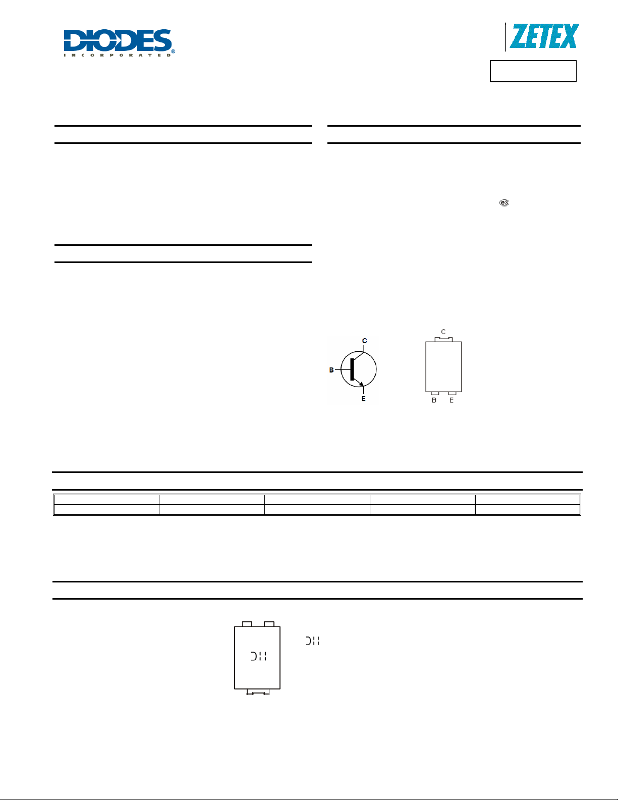
PowerDI®5
Top View Bottom View Pin-out diagram Device Schematic
Product Line o
Diodes Incorporated
DXT5551P5
160V NPN HIGH VOLTAGE TRANSISTOR
PowerDI
Mechanical Data
• Case: PowerDI®5
• Case Material: Molded Plastic, “Green” Molding Compound.
UL Flammability Classification Rating 94V-0
• Moisture Sensitivity: Level 1 per J-STD-020
• Terminals: Finish – Matte Tin annealed over Copper leadframe.
Solderable per MIL-STD-202, Method 208
• Weight: 0.093 grams (approximate)
®
5
Ordering Information (Note 3)
Product Marking Reel size (inches) Tape width (mm) Quantity per reel
DXT5551P5-13 DXT5551 13 16 5,000
Notes: 1. No purposefully added lead.
2. Halogen and Antimony Free. Diodes Inc’s “Green” Policy can be found on our website at http://www.diodes.com
3. For packaging details, go to our website at http://www.diodes.com
Marking Information
PowerDI is a registered trademark of Diodes Incorporated.
DXT5551
YYWWK
DXT5551P5
Document number: DS32066 Rev. 3 - 2
DXT5551 = Product Type Marking Code
= Manufacturers’ Code Marking
K = Factory Designator
YYWW = Date Code Marking
YY = Last Two Digits of Year (ex: 09 for 2009)
WW = Week code (01 - 53)
1 of 7
www.diodes.com
November 2010
© Diodes Incorporated
Page 2
A
f
θ
θ
θ
θ
Product Line o
Diodes Incorporated
DXT5551P5
Maximum Ratings @T
= 25°C unless otherwise specified
A
Characteristic Symbol Value Unit
Collector-Base Voltage
Collector-Emitter Voltage
Emitter-Base Voltage
Continuous Collector Current
V
CBO
V
CEO
V
EBO
I
C
Thermal Characteristics @T
= 25°C unless otherwise specified
A
Characteristic Symbol Value Unit
Power Dissipation (Note 4)
Thermal Resistance, Junction to Ambient Air (Note 4)
Power Dissipation (Note 5)
Thermal Resistance, Junction to Ambient Air (Note 5)
Power Dissipation (Note 6)
Thermal Resistance, Junction to Ambient Air (Note 6)
Thermal Resistance, Junction to Collector Terminal
Operating and Storage Temperature Range
ADVANCE INFORMATION
Notes: 4. Device mounted on 1.6mm FR-4 PCB, single sided 2 oz. copper, collector pad dimensions 50mm x 50mm.
5. Device mounted on 1.6mm FR-4 PCB, single sided 1 oz. copper, collector pad dimensions 25mm x 25mm.
6. Device mounted on 1.6mm FR-4 PCB, single sided 1 oz. copper, minimum recommended pad layout.
P
D
R
JA
P
D
R
JA
P
D
R
JA
R
JT
, T
T
J
STG
180 V
160 V
6 V
600 mA
2.25 W
55.5 °C/W
1.28 W
97.4 °C/W
0.7 W
179 °C/W
30 °C/W
-55 to +150 °C
PowerDI is a registered trademark of Diodes Incorporated.
DXT5551P5
Document number: DS32066 Rev. 3 - 2
2 of 7
www.diodes.com
November 2010
© Diodes Incorporated
Page 3
A
f
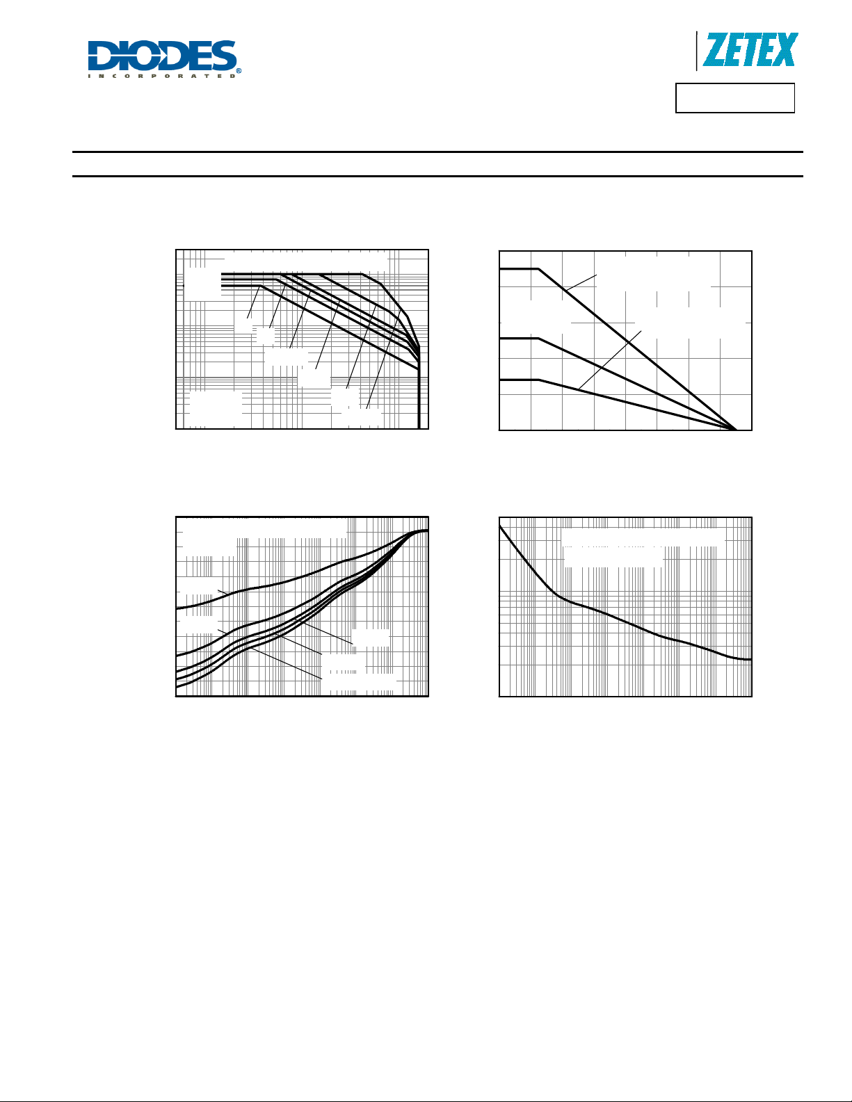
Thermal Characteristics
Product Line o
Diodes Incorporated
DXT5551P5
1
V
Limited
100m
10m
Collector Current (A)
C
I
1m
ADVANCE INFORMATION
Mounted on 50X50mm pad, 2 oz copper
CE(sat)
DC
1s
100ms
10ms
Singl e Pulse
T
=25°C
amb
1ms
100µs
1 10 100
VCE Collector-Emitter Voltage (V)
Safe Operating A rea
2.0
25X25mm Pad
1.5
1oz copper
1.0
0.5
0.0
0 20 40 60 80 100 120 140 160
Max Power Dissipati on (W)
Temperature (°C)
Derating Curve
Mounted on 50X50mm pad
2 oz copper
Minimum recomended pad
1oz copper
60
2.5
Mounted on 50X50mm pad, 2 oz copper
T
amb
D=0.5
=25°C
50
40
10
Mounted on 50X50mm pad, 2 oz copper
Singl e Pulse T
amb
=25°C
30
D=0.2
20
D=0.1
10
0
100µ 1m 10m 100m 1 10 100 1k
Thermal Resistan ce (°C/W)
Pulse Width (s)
Transient Thermal Impedance
D=0.05
Single Pulse
Maximum Power (W)
1
100µ 1m 10m 100m 1 10 100 1k
Pulse Width (s)
Pulse Power Dissipation
PowerDI is a registered trademark of Diodes Incorporated.
DXT5551P5
Document number: DS32066 Rev. 3 - 2
3 of 7
www.diodes.com
November 2010
© Diodes Incorporated
Page 4

A
f
(d)
(r)
(s)
(f)
Product Line o
Diodes Incorporated
DXT5551P5
Electrical Characteristics @T
= 25°C unless otherwise specified
A
Characteristic Symbol Min Typ Max Unit Test Condition
Collector-Base Breakdown Voltage
Collector-Emitter Breakdown Voltage (Note 7)
Emitter-Base Breakdown Voltage
Collector Cutoff Current
Collector-Emitter Saturation Voltage (Note 7)
Base-Emitter Saturation Voltage (Note 7)
DC Current Gain (Note 7)
Transition Frequency
Output Capacitance (Note 7)
Delay Time
Rise Time
Storage Time
ADVANCE INFORMATION
Delay Time
Notes: 7. Pulse Test: Pulse width ≤300μs. Duty cycle ≤2.0%.
BV
BV
BV
I
CBO
V
CE(sat)
V
BE(sat)
h
C
t
t
t
t
CBO
CEO
EBO
FE
f
T
obo
180 270
160 200
6.0 7.85
80
80
30
−
−
<1
−
−
−
−
−
65
115
760
840
130
145
65
130
− −
−
−
−
−
95
64
1256
140
−
−
−
50
−
50
150
200
1000
1200
−
250
−
−
6 pF
−
−
−
−
V
I
= 100μA
C
V
I
= 1mA
C
V
I
= 10μA
E
nA
V
= 120V
CB
μA
V
= 120V, TA = 100°C
CB
= 10mA, IB = 1mA
I
mV
C
mV
mV
mV
= 50mA, IB = 5mA
I
C
= 10mA, IB = 1mA
I
C
I
= 50mA, IB = 5mA
C
V
CE
−
V
CE
= 5V, IC = 1mA
= 5V, IC = 10mA
VCE = 5V, IC = 50mA
V
MHz
CE
f = 100MHz
= 10V, f = 1MHz
V
CB
ns
Ns
ns
= 510V, IC = 10mA,
V
CC
I
= IB2 = 1mA
B1
ns
= 10V, IC = 10mA,
PowerDI is a registered trademark of Diodes Incorporated.
DXT5551P5
Document number: DS32066 Rev. 3 - 2
4 of 7
www.diodes.com
November 2010
© Diodes Incorporated
Page 5

A
f
Typical Characteristics
Product Line o
Diodes Incorporated
DXT5551P5
1
Tamb=25°C
(V)
100m
CE(SAT)
V
IC/IB=10
1m 10m 100m
IC/IB=50
IC/IB=20
IC Collector Curre nt (A)
V
CE(SAT)
v I
C
ADVANCE INFORMATION
1.6
150°C
1.4
1.2
100°C
1.0
0.8
25°C
0.6
0.4
Normalised Gain
0.2
0.0
100µ 1m 10m 100m
-55°C
IC Collector Current (A)
hFE v I
Ta=25°C
VCE=5V
200
)
150
100
50
Typical Gain (h
0
C
0.7
IC/IB=10
0.6
0.5
0.4
(V)
0.3
CE(SAT)
0.2
V
0.1
0.0
10m 100m
-55°C
150°C
100°C
25°C
IC Collector Cu rre nt (A)
V
1.2
IC/IB=10
1.0
FE
0.8
25°C
CE(SAT)
-55°C
v I
C
(V)
0.6
BE(SAT)
V
0.4
0.2
1m 10m 100m
100°C
150°C
IC Collector Cu rre nt (A)
V
BE(SAT)
v I
C
VCE=5V
1.0
25°C
0.8
-55°C
(V)
0.6
BE(ON)
V
0.4
1m 10m 100m
150°C
100°C
IC Collector Cu rre nt (A)
V
PowerDI is a registered trademark of Diodes Incorporated.
DXT5551P5
Document number: DS32066 Rev. 3 - 2
BE(ON)
v I
C
5 of 7
www.diodes.com
November 2010
© Diodes Incorporated
Page 6

A
f
Package Outline Dimensions
ADVANCE INFORMATION
D
b2
e
b1
Product Line o
Diodes Incorporated
DXT5551P5
A
A2
E
b1
E1
W
A2
D2
L
E2
L1
PowerDI®5
Dim Min Max
A 1.05 1.15
A2 0.33 0.43
b1 0.80 0.99
b2 1.70 1.88
D 3.90 4.05
D2 3.054 Typ
E 6.40 6.60
e 1.84 Typ
E1 5.30 5.45
E2 3.549 Typ
L 0.75 0.95
L1 0.50 0.65
W 1.10 1.41
All Dimensions in mm
Suggested Pad Layout
Y1
(2x)
X
Y
X1
(2x)
C
G
Dimensions Value (in mm)
C 1.840
G 0.852
X 3.360
X1 1.390
Y 4.860
Y1 1.400
PowerDI is a registered trademark of Diodes Incorporated.
DXT5551P5
Document number: DS32066 Rev. 3 - 2
6 of 7
www.diodes.com
November 2010
© Diodes Incorporated
Page 7

A
f
Product Line o
DIODES INCORPORATED MAKES NO WARRANTY OF ANY KIND, EXPRESS OR IMPLIED, WITH REGARDS TO THIS DOCUMENT,
INCLUDING, BUT NOT LIMITED TO, THE IMPLIED WARRANTIES OF MERCHANTABILITY AND FITNESS FOR A PARTICULAR PURPOSE
(AND THEIR EQUIVALENTS UNDER THE LAWS OF ANY JURISDICTION).
Diodes Incorporated and its subsidiaries reserve the right to make modifications, enhancements, improvements, corrections or other changes
without further notice to this document and any product described herein. Diodes Incorporated does not assume any liability arising out of the
application or use of this document or any product descri bed herein; neither does Diodes Incorporated convey any license under its patent or
trademark rights, nor the rights of others. Any Customer o r user of this document or products described he rein in such applicati ons shall assume
all risks of such use and will agree to hold Diodes Incorporated and all the companies whose products are represented on Diodes Incorporated
website, harmless against all damages.
Diodes Incorporated does not warrant or accept any liability whatsoever in respect of any products purchased through unauthorized sales channel.
Should Customers purchase or use Diodes Incorporated products for any unintende d or unauthorized applicati on, Customers shall indemnif y and
hold Diodes Incorporated and its representatives harmless against all claims, damages, expenses, and attorney fees arising out of, directly or
indirectly, any claim of personal injury or death associated with such unintended or unauthorized application.
Products described herein may be covered by one or more United States, international or foreign patents pending. Product names and marki ngs
noted herein may also be covered by one or more United States, international or foreign trademarks.
Diodes Incorporated products are specifically not authorized for use as cri tical components in life support devi ces or systems without the express
ADVANCE INFORMATION
written approval of the Chief Executive Officer of Diodes Incorporated. As used herein:
A. Life support devices or systems are devices or systems which:
1. are intended to implant into the body, or
labeling can be reasonably expected to result in significant injury to the user.
B. A critical component is any component in a life support device or system whose failure to perform can be reasonably expected to cause the
failure of the life support device or to affect its safety or effectiveness.
Customers represent that they have all necessary expertise in the safety and regulatory ramifications of their life support devices or systems, and
acknowledge and agree that they are solely responsible for all legal, regulatory and safety-related requirements concerning the ir pro ducts and an y
use of Diodes Incorporated products in such safety-critical, life support devices or systems, notwithstanding any devices- or systems-related
information or support that may be provided by Diodes Incorporated. Further, Customers must fully indemnify Diodes Incorporated and its
representatives against any damages arising out of the use of Diodes Incorporated products in such safety-critical, life support devices or systems.
Copyright © 2010, Diodes Incorporated
www.diodes.com
2. support or sustain life and whose failure to perform when properly used in accordance with instructions for use provided in the
IMPORTANT NOTICE
LIFE SUPPORT
Diodes Incorporated
DXT5551P5
PowerDI is a registered trademark of Diodes Incorporated.
DXT5551P5
Document number: DS32066 Rev. 3 - 2
7 of 7
www.diodes.com
November 2010
© Diodes Incorporated
 Loading...