

Page 1
Features
• Epitaxial Planar Die Construction
• Selectively Paired NPN Transistors & Zener Diodes for Series
Pass Voltage Regulator Circuits
• Ideally Suited for Automated Assembly Processes
• Lead, Halogen and Antimony Free, RoHS Compliant (Note 1)
• "Green" Device (Note 2)
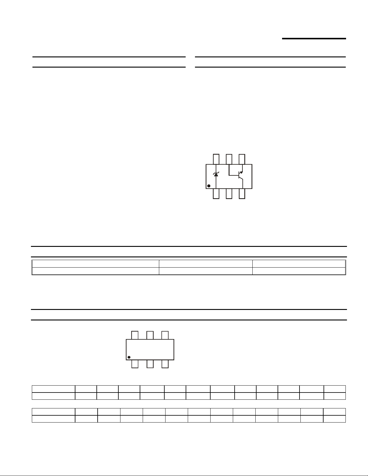
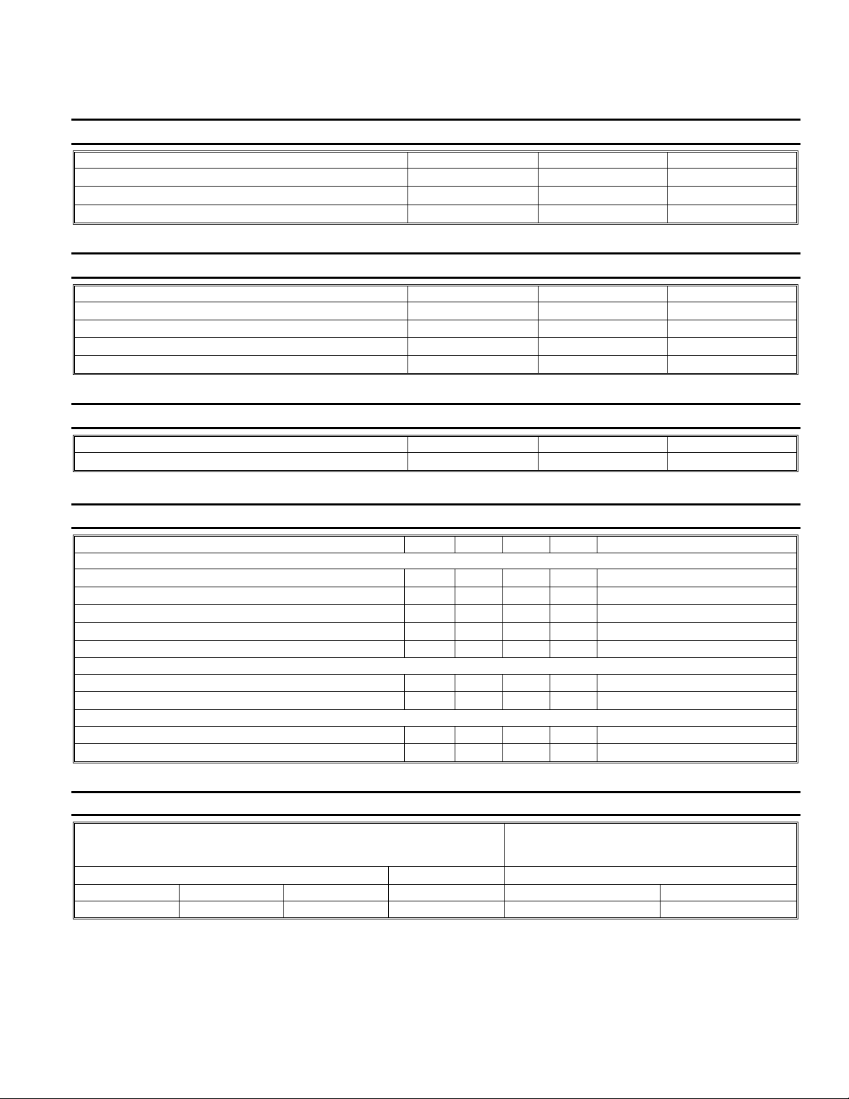
SOT363
Top View
DVR5V0W
COMPLEX ARRAY FOR VOLTAGE REGULATORS
Mechanical Data
• Case: SOT363
• Case Material: Molded Plastic, "Green" Molding Compound.
UL Flammability Classification Rating 94V-0
• Moisture Sensitivity: Level 1 per J-STD-020
• Terminals: Matte Tin Finish annealed over Alloy 42 leadframe
(Lead Free Plating). Solderable per MIL-STD-202, Method 208
• Terminal Connections: See Diagram
• Weight: 0.006 grams (approximate)
K
1
A
1
Top View
Pin Configuration
E
B
1
1
NC
C
1
Ordering Information (Note 3)
Device Packaging Shipping
DVR5V0W-7 SOT363 3000/Tape & Reel
Notes: 1. No purposefully added lead.
2. Diodes Inc’s “Green” policy can be found on our website at http://www.diodes.com/products/lead_free/index.php.
3. For packaging details, go to our website at http://www.diodes.com/datasheets/ap02007.pdf.
Marking Information
Date Code Key
Year 2004 2005 2006 2007 2008 2009 2010 2011 2012 2013 2014 2015
Code R S T U V W X Y Z A B C
Month Jan Feb Mar Apr May Jun Jul Aug Sep Oct Nov Dec
Code 1 2 3 4 5 6 7 8 9 O N D
VR04
VR04 = Product Type Marking Code
YM = Date Code Marking
Y = Year ex: Y = 2011
YM
M = Month ex: 9 = September
DVR5V0W
Document number: DS30578 Rev. 6 - 2
1 of 5
www.diodes.com
© Diodes Incorporated
July 2011
Page 2
Maximum Ratings, Total Device @T
= 25°C unless otherwise specified
A
Characteristic Symbol Value Unit
Power Dissipation (Note 4)
Thermal Resistance, Junction to Ambient (Note 4)
Operating and Storage Temperature Range
Maximum Ratings, NPN Transistor @T
= 25°C unless otherwise specified
A
R
Tj, T
Characteristic Symbol Value Unit
Collector-Base Voltage
Collector-Emitter Voltage
Emitter-Base Voltage
V
V
V
Collector Current - Continuous (Note 4)
Maximum Ratings, Zener Element @T
= 25°C unless otherwise specified
A
Characteristic Symbol Value Unit
Forward Voltage @ IF = 10mA VF
Electrical Characteristics, NPN Transistor @T
= 25°C unless otherwise specified
A
Pd
θ
CBO
CEO
EBO
IC
JA
STG
200 mW
625
-55 to +150
45 V
18 V
5 V
°C/W
°C
1 A
0.9 V
Characteristic Symbol Min Max Unit Test Condition
OFF CHARACTERISTICS (Note 5)
Collector-Base Breakdown Voltage
Collector-Emitter Breakdown Voltage
Emitter-Base Breakdown Voltage
Collector Cutoff Current
Emitter Cutoff Current
V
(BR)CBO
V
(BR)CEO
V
(BR)EBO
I
CBO
I
EBO
45
18
⎯
⎯
⎯
⎯
5
⎯
1
1
V
IC = 100μA, IE = 0
V
IC = 1mA, IB = 0
V
IE = 100μA, IC = 0
μA
VCB = 40V, IE = 0
μA
V
EB
= 4V, IC = 0
ON CHARACTERISTICS (Note 5)
DC Current Gain
Collector-Emitter Saturation Voltage
hFE
V
CE(SAT)
150 800
⎯
0.5 V
⎯
IC = 100mA, V
IC = 300mA, IB = 30mA
CE
= 1V
SMALL SIGNAL CHARACTERISTICS
Output Capacitance
C
Current Gain-Bandwidth Product
Electrical Characteristics, Zener Element @T
Zener Voltage Range
(Note 6)
⎯
obo
fT
100
= 25°C unless otherwise specified
A
8 pF
MHz
⎯
VCB = 10V, f = 1.0MHz, IE = 0
VCB = 10V, IE = 50mA, f = 100MHz
Maximum Reverse
Leakage Current
(Note 5)
VZ @ IZT IZT IR @ VR
Nom (V) Min (V) Max (V) mA
μA
V
5.1 4.85 5.36 0.05 5 3
Notes: 4. Part mounted on FR-4 board with recommended pad layout, which can be found on our website at http://www.diodes.com/da tashee ts/ap02001.pdf.
5. Short duration pulse test used to minimize self-heating effect.
DVR5V0W
Document number: DS30578 Rev. 6 - 2
6. Nominal Zener voltage is measured with the device junction in thermal equilibrium at T
2 of 5
www.diodes.com
= 30°C ±1°C.
T
July 2011
© Diodes Incorporated
Page 3

P, P
OWER
P
T
O
C CUR
R
T
G
C, OUTPU
T CAPACITAN
C
F
C
O
CTO
R
T
TER
200
(Note 4)
1,000
150
N (mW)
I
A
100
AIN
EN
100
DISSI
d
)
E (p
OBO
100
50
10
0
0
25 50
T , AMBIENT TEMPERATURE (°C)
A
75
100 125
Fig. 1 Max Pow er Dissipa t ion vs.
Ambien t Temperat ur e (Total Device)
1
0.1
V , COLLECTOR-BASE VOLTAGE (V)
CB
1
Fig. 3 Typical Output Capacitance vs.
Collector-Base Voltage (NPN Transistor)
10
150
175
200
100
FE
h, D
1
0.0001 .001 .01 1 10.1
I , COLLECTOR CURRENT (A)
C
Fig. 2 Typical DC Current Gain vs.
Collector Current (NPN Tra nsi stor)
1,000
(mV)
-EMI
100
LLE
10
CE (SAT)
SATURATION VOLT AGE
V,
1
0.0001
.001
I , COLLECTOR CURRENT (A)
C
Fig. 4 Typical Collector Saturation Voltage vs.
Collector Current (NPN Transistor)
.01
V = 1.0V
CE
.1 1
10
V , ZENER VOL TAGE (V)
DVR5V0W
Document number: DS30578 Rev. 6 - 2
Fig. 5 Typical
Z
Zener Breakdown Characteristics
3 of 5
www.diodes.com
July 2011
© Diodes Incorporated
Page 4

Sample Applications
Notes: 7. Resistor R1 not included.
8. Typical performance shown is under setup and operating conditions specified in the sample applications.
9. Recommended V
VCC = 6.0V
(min) ~ Vo(nom) + 1V.
CC
R1 = 560R
Z1
DVR5V0W
Q1
Vo(nom) = 5.0V
R Load
Sample Application for DVR5V0W:
= 6.0V R1= 560Ω
V
CC
Vo(nom) = 5.0V I
Iq(typical) = 0.5mA @ I
= 100mA
O
= 0mA
O
Typical Vreg(load) = 0.2V from Io = 100mA to 0mA
Package Outline Dimensions
K
J
A
SOT363
Dim Min Max
A 0.10 0.30
B C
B 1.15 1.35
C 2.00 2.20
D 0.65 Typ
F 0.40 0.45
H 1.80 2.20
H
J 0 0.10
K 0.90 1.00
M
D
L
F
L 0.25 0.40
M 0.10 0.22
0° 8°
α
All Dimensions in mm
Suggested Pad Layout
G
Z
Y
X
C2
C2
C1
Dimensions Value (in mm)
Z 2.5
G 1.3
X 0.42
Y 0.6
C1 1.9
C2 0.65
DVR5V0W
Document number: DS30578 Rev. 6 - 2
4 of 5
www.diodes.com
July 2011
© Diodes Incorporated
Page 5

DIODES INCORPORATED MAKES NO WARRANTY OF ANY KIND, EXPRESS OR IMPLIED, WITH REGARDS TO THIS DOCUMENT,
INCLUDING, BUT NOT LIMITED TO, THE IMPLIED WARRANTIES OF MERCHANTABILITY AND FITNESS FOR A PARTICULAR PURPOSE
(AND THEIR EQUIVALENTS UNDER THE LAWS OF ANY JURISDICTION).
Diodes Incorporated and its subsidiaries reserve the right to make modifications, enhancements, improvements, corrections or other changes
without further notice to this document and any product described herein. Diodes Incorporated does not assume any liability arising out of the
application or use of this document or any product described herein; neither does Diodes Incorporated convey any license under its patent or
trademark rights, nor the rights of others. Any Customer or user of this document or products described herein in such applications shall assume
all risks of such use and will agree to hold Diodes Incorporated and all the companies whose products are represented on Diodes Incorporated
website, harmless against all damages.
Diodes Incorporated does not warrant or accept any liability whatsoever in respect of any products purchased through unauthorized sales channel.
Should Customers purchase or use Diodes Incorporated products for any unintended or unauthorize d application, Customers shall indemnify and
hold Diodes Incorporated and its representatives harmless against all claims, damages, expenses, and attorney fees arising out of, directly or
indirectly, any claim of personal injury or death associated with such unintended or unauthorized application.
Products described herein may be covered by one or more United States, international or foreign patents pending. Product names and markings
noted herein may also be covered by one or more United States, international or foreign trademarks.
Diodes Incorporated products are specifically not authorized for use as critical components in life support devices or systems without the express
written approval of the Chief Executive Officer of Diodes Incorporated. As used herein:
A. Life support devices or systems are devices or systems which:
1. are intended to implant into the body, or
2. support or sustain life and whose failure to perform when properly used in accordance with instructions for use provided in the
labeling can be reasonably expected to result in significant injury to the user.
B. A critical component is any component in a life support device or system whose failure to perform can be reasonably expected to cause the
failure of the life support device or to affect its safety or effectiveness.
Customers represent that they have all necessary expertise in the safety and regulatory ramifications of their life support devices or systems, and
acknowledge and agree that they are solely responsible for all legal, regulatory and safety-related requirements concerning their products and any
use of Diodes Incorporated products in such safety-critical, life support devices or systems, notwithstanding any devices- or systems-related
information or support that may be provided by Diodes Incorporated. Further, Customers must fully indemnify Diodes Incorporated and its
representatives against any damages arising out of the use of Diodes Incorporated products in such safety-critical, life support devices or systems.
Copyright © 2011, Diodes Incorporated
www.diodes.com
IMPORTANT NOTICE
LIFE SUPPORT
DVR5V0W
Document number: DS30578 Rev. 6 - 2
5 of 5
www.diodes.com
July 2011
© Diodes Incorporated
 Loading...