Diodes DT2042-04SO User Manual

Features
Low Clamping Voltage
Typical 9V at 10A 100ns, TLP
Typical 9V at 10A 8μs/20μs
IEC 61000-4-2 (ESD): Air – ±30kV, Contact – ±30kV
IEC 61000-4-4 (EFT): 60A(5/50ns, I/O to V
IEC 61000-4-5 (Lightning): ±10A
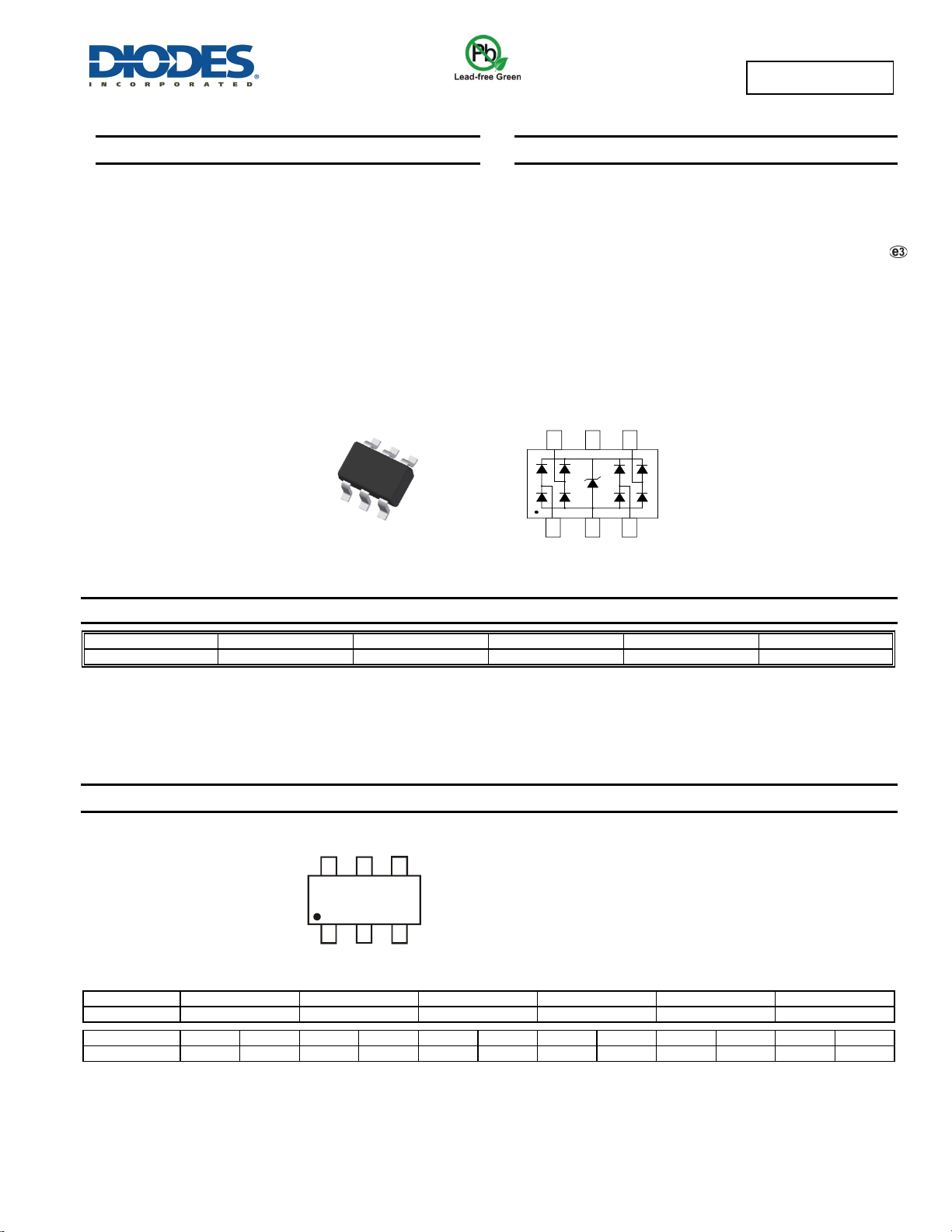
4 Channels of ESD protection
Low Channel Input Capacitance of 1.2pF Typical
TLP Dynamic Resistance: 0.25Ω
Typically Used for High Speed Ports such as USB 2.0,
IEEE1394, VGA, Laptop and Personal Computers,
Flat Panel Displays, Video Graphics Displays, SIM Ports
Totally Lead-Free & Fully RoHS Compliant (Notes 1 & 2)
Halogen and Antimony Free. “Green” Device (Note 3)
ADVANCE INFORMATION
)
ss
SOT26
Top View
DT2042-04SO
4 CHANNEL LOW CAPACITANCE TVS DIODE ARRAY
Mechanical Data
Case: SOT26
Case Material: Molded Plastic, “Green” Molding Compound.
UL Flammability Classification Rating 94V-0
Moisture Sensitivity: Level 1 per J-STD-020
Terminals: Matte Tin Finish annealed over Copper leadframe
(Lead Free Plating). Solderable per MIL-STD-202, Method 208
Weight: 0.016 grams (approximate)
NC
I/O 4
6
1
I/O 1
Device Schematic
I/O 3
4
5
3
2
V
I/O 2
SS
Ordering Information (Note 4)
Product Compliance Marking Reel Size (inches) Tape Width (mm) Quantity per Reel
DT2042-04SO-7 Standard BC5 7 8 3,000/Tape & Reel
Notes: 1. No purposely added lead. Fully EU Directive 2002/95/EC (RoHS) & 2011/65/EU (RoHS 2) compliant.
2. See http://www.diodes.com/quality/lead_free.html for more information about Diodes Incorporated’s definitions of Halogen- and Antimony-free, "Green"
and Lead-free.
3. Halogen- and Antimony-free "Green” products are defined as those which contain <900ppm bromine, <900ppm chlorine (<1500ppm total Br + Cl) and
<1000ppm antimony compounds.
4. For packaging details, go to our website at http://www.diodes.com/products/packages.html.
Marking Information
BC5
A17
YM
BC5 = Product Type Marking Code
YM = Date Code Marking
Y = Year (ex: A = 2013)
M = Month (ex: 9 = September)
Date Code Key
Year 2013 2014 2015 2016 2017 2018
Code A B C D E F
Month Jan Feb Mar Apr May Jun Jul Aug Sep Oct Nov Dec
Code 1 2 3 4 5 6 7 8 9 O N D
DT2042-04SO
Document number: DS36296 Rev. 2 - 2
1 of 5
www.diodes.com
August 2013
© Diodes Incorporated

V
V
P
P
U
RATING
O
R
O
OLT
G
T
RIG
GER
OLTAG
Maximum Ratings (@T
Characteristic Symbol
Peak Pulse Current, per IEC 61000-4-5
Peak Pulse Power, per IEC 61000-4-5
Operating Voltage (DC)
ESD Protection – Contact Discharge, per IEC61000-4-2
ESD Protection – Air Discharge, per IEC 61000-4-2
Operating Temperature
Storage Temperature
= +25°C, unless otherwise specified.)
A
I
PP
P
PP
V
DC
V
ESD_contact
V
ESD_air
T
OP
T
STG
alue Unit Conditions
±10 A
105 W
5.5 V
±30 kV
±30 kV
-55 to +85 °C
-55 to +150 °C
DT2042-04SO
I/O to VSS, 8/20 μs
I/O to VSS, 8/20 μs
I/O to VSS
I/O to VSS
I/O to VSS
—
—
Thermal Characteristics
Characteristic Symbol
Power Dissipation Typical (Note 5)
Thermal Resistance, Junction to Ambient Typical (Note 5)
Electrical Characteristics (@T
Characteristic Symbol Min Typ Max Unit Test Conditions
Reverse Working Voltage
ADVANCE INFORMATION
Reverse Current(Note6)
Reverse Breakdown Voltage
Forward Clamping Voltage
Holding Voltage
Trigger Voltage
Reverse Clamping Voltage (Note 7)
Reverse Clamping Voltage (Note 7)
ESD Clamping Voltage
Dynamic Resistance
Channel Input Capacitance C
Variation of Channel Input Capacitance
Notes: 5. Device mounted on FR-4 PCB pad layout (2oz copper) as shown on Diodes, Inc. suggested pad layout AP02001, which can be found on our website
6. Short duration pulse test used to minimize self-heating effect.
7. Clamping voltage value is based on an 8x20µs peak pulse current (I
at http://www.diodes.com.
= +25°C, unless otherwise specified.)
A
V
V
V
V
V
R
C
RWM
I
R
V
BR
V
F
V
H
TRIG
C_5A
C_10A
ESD
DIF
I/O
I/O
— —
— —
6
-1.0 -0.8
5.5
—
—
—
—
—
—
—
—
— —
9 9.5 V
7.5
9 10.5 V
9
0.25
1.2 1.5 pF
0.02
P
D
R
θJA
5.5 V
1 μA
9 V
—
—
—
—
—
) waveform.
pp
E,
V
V
V
V
Ω
pF
9.5
alue Unit
300 mW
417 °C/W
SS
I/O to V
VR = 5V, any I/O to VSS
= 1mA, I/O to VSS
I
R
= -15mA, I/O to VSS
I
F
—
—
= 5A, I/O to VSS, 8/20 μs
I
PP
= 10A, I/O to VSS, 8/20 μs
I
PP
TLP, 10A, tp = 100 ns, I/O to V
TLP, 10A, tp = 100 ns, I/O to V
= 2.5V, f = 1MHz
V
R
Vss = 0V,I/O = 2.5V, f =1MHz, T=25°C ,
I/O_x to V
– I/O_y to VSS
SS
, per Fig. 7
SS
SS
F
IN %
LSE DE
PEAK POWER OR CURRENT
EAK
T , AMBIENT TEMPERATURE (°C)
A
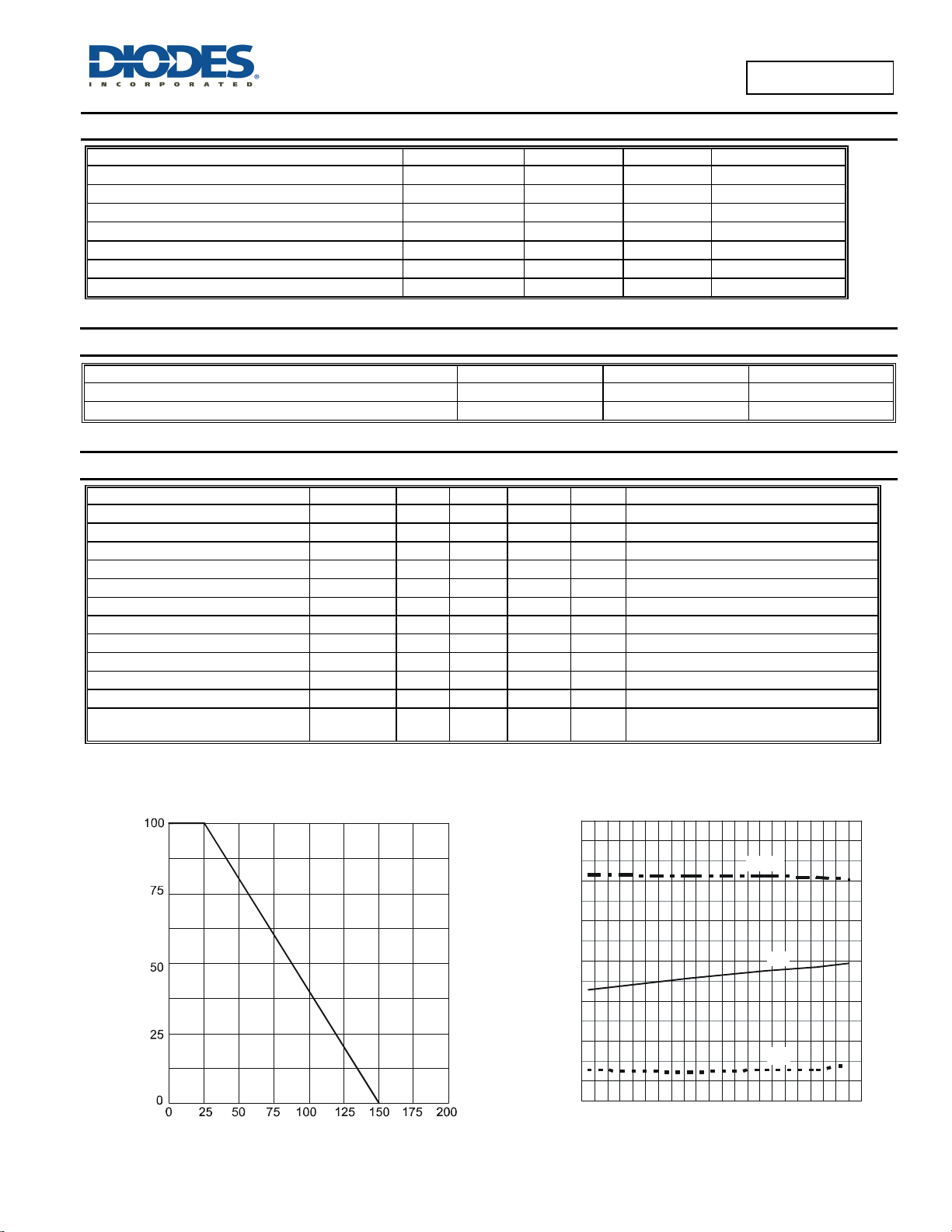
Figure 1 Pulse Derating Curve
DT2042-04SO
Document number: DS36296 Rev. 2 - 2
2 of 5
www.diodes.com
9.0
V
8.5
8.0
E,
A
7.5
7.0
HOLDING VOLTAGE (V)
WN V
6.5
EAKD
B
6.0
-60 -40 -20 0 20 40 60 80 100 120 140 160
T , AMBIENT TEMPERATURE(°C)
A
Figure 2 BV, Trigger Voltage, Holding Voltage vs.
Ambient Temperature
VTRIG
BV
VH
© Diodes Incorporated
August 2013
 Loading...