

Page 1
COMPLEMENTARY DUAL SMALL SIGNAL SURFACE MOUNT TRANSISTOR
Features
• Epitaxial Planar Die Construction
• Ideally Suited for Automated Assembly Processes
• Lead, Halogen and Antimony Free, RoHS Compliant (Note 1)
• “Green” Device (Note 2)
• Ultra Small Package
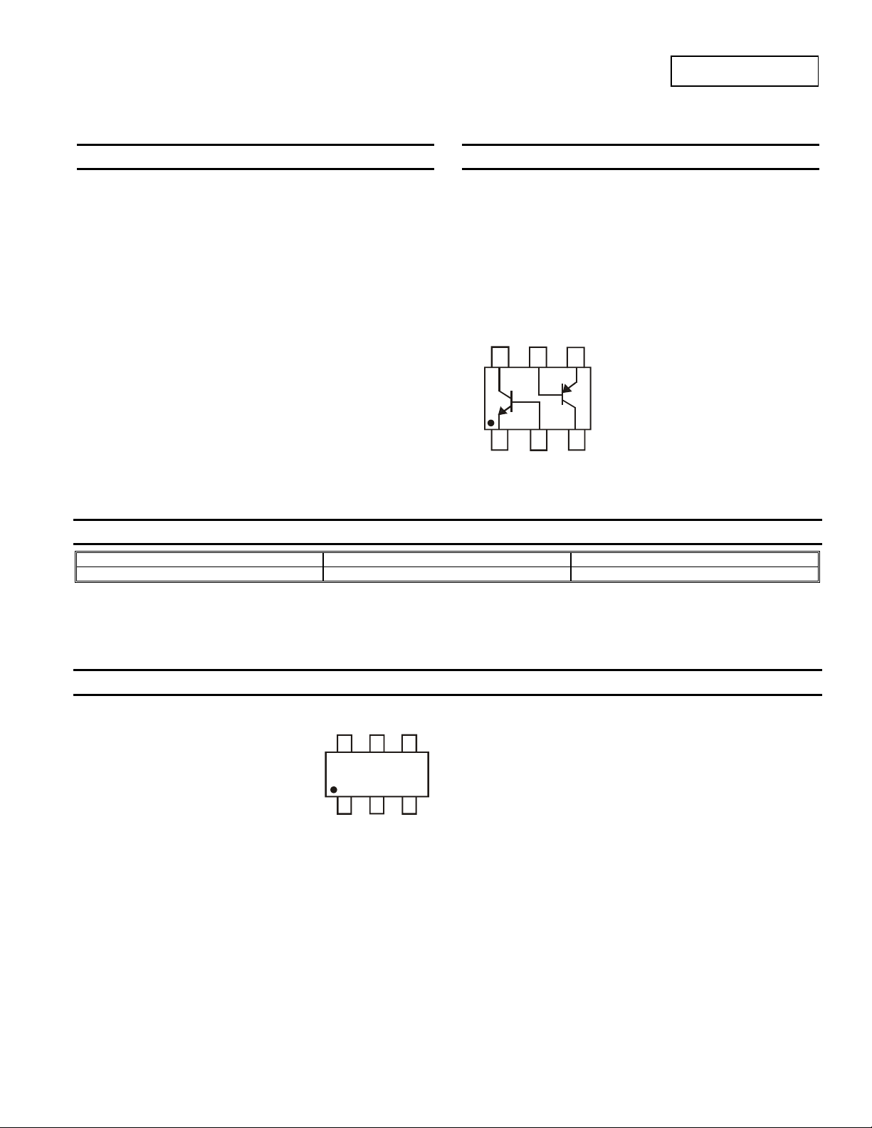
SOT-963
DST847BPDP6
Mechanical Data
• Case: SOT-963
• Case Material: Molded Plastic, “Green” Molding Compound.
UL Flammability Classification Rating 94V-0
• Moisture Sensitivity: Level 1 per J-STD-020
• Terminals: Finish ⎯ Matte Tin annealed over Copper leadframe.
Solderable per MIL-STD-202, Method 208
• Weight: 0.0027 grams (approximate)
6
Q1
Device SchematicTop View
4
5
Q2
2
31
Ordering Information
Device Packaging Shipping
DST847BPDP6-7 SOT-963 10,000/Tape & Reel
Notes: 1. No purposefully added lead. Halogen and Antimony Free.
2. Diodes Inc’s “Green” Policy can be found on our website at http://www.diodes.com
Marking Information
TC
TC = Product Type Marking Code
DST847BPDP6
Document number: DS32036 Rev. 1 - 2
1 of 8
www.diodes.com
January 2010
© Diodes Incorporated
Page 2
θ
T
R
T T
HER
R
TANC
P
P
T
RAN
N
T P
OWER
P
P
OWER
P
TIO
N
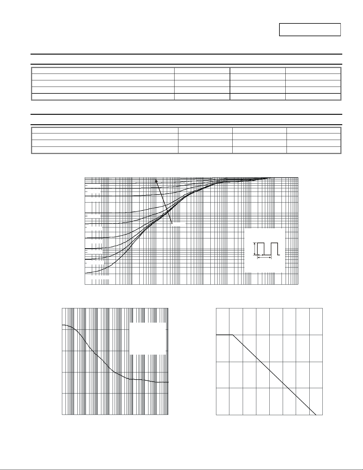
Maximum Ratings @T
= 25°C unless otherwise specified
A
Characteristic Symbol Value Unit
Collector-Base Voltage
Collector-Emitter Voltage
Emitter-Base Voltage
Collector Current - Continuous (Note 3)
Thermal Characteristics
Characteristic Symbol Value Unit
Power Dissipation (Note 3)
Thermal Resistance, Junction to Ambient (Note 3)
Operating and Storage Temperature Range
Notes: 3. Device mounted on FR-4 PCB with minimum recommended pad layout.
1
D = 0.7
E
D = 0.5
D = 0.3
DST847BPDP6
V
CBO
V
CEO
V
EBO
I
C
P
D
R
JA
T
, T
J
STG
50(-50) V
45(-45) V
6.0(-5.0) V
100 (-100) mA
250 mW
500 °C/W
-55 to +150 °C
1,000
(W)
100
SIE
10
ESIS
0.1
D = 0.1
MAL
0.01
ANSIEN
r(t),
D = 0.05
D = 0.02
D = 0.01
D = 0.005
D = Single Pulse
D = 0.9
R (t) = r(t) *
θ
JA
R = 370°C/W
JA
P(pk)
t
1
t
2
T - T = P * R (t)
JA JA12θ
Duty Cycle, D = t /t
R
θθJA
0.001
0.000001 0.0001 0.001 0.01 0.1 1 10 100 1,000
0.00001
t , PULSE DURA TION TIME (s)
1
Fig. 1 Transi ent Thermal Respo nse
0.4
Single Pulse
R (t) = r(t) *
θ
JA
R = 370°C/W
T - T = P * R (t)
JA JA12θ
Duty Cycle, D = t /t
R
JA
θθJA
0.3
(W)
Note 3
A
0.2
1
DISSI
EAK
0.1
,
0.1
D
(pk),
0.01
0.00001 0.001 0.1 10 1,000
t , PULSE DURATION TIME (s)
1
Fig. 2 Single Pulse Maximum Power Dissipation
0
0 20 40 60 80 100 120 140 160
T , AMBIENT TEMPERATURE ( C)
A
°
Fig. 3 Pow er Dissipat ion vs. Ambient Temperat ur e
DST847BPDP6
Document number: DS32036 Rev. 1 - 2
2 of 8
www.diodes.com
January 2010
© Diodes Incorporated
Page 3
(BR)
Electrical Characteristics – Q1 NPN Transistor @T
Characteristic (Note 4) Symbol Min Typical Max Unit Test Condition
Collector-Base Breakdown Voltage
Collector-Emitter Breakdown Voltage
Collector-Emitter Breakdown Voltage
Emitter-Base Breakdown Voltage
Collector-Base Cutoff Current
DC Current Gain
Collector-Emitter Saturation Voltage
Base-Emitter Saturation Voltage
Base-Emitter Voltage
Current Gain-Bandwidth Product
Collector-Base Capacitance
Notes: 4. Short duration pulse test used to minimize self-heating effect
V
V
(BR)CES
V
(BR)CEO
V
(BR)EBO
I
CBO
h
V
CE(sat)
V
BE(sat)
V
BE(on)
C
f
FE
T
cbo
CBO
50
50
45
6
-
100
200
-
-
-
-
580
100
-
DST847BPDP6
Document number: DS32036 Rev. 1 - 2
3 of 8
www.diodes.com
= 25°C unless otherwise specified
A
150
150
65
8.35
-
220
300
50
122
760
880
650
725
175
1.5
- V
- V
- V
- V
15 nA
-
470
125
300
1000
1100
750
800
-
mV
mV
mV
- MHz
- pF
IC = 10μA, IB = 0
IC = 10μA, IB = 0
IC = 1mA, IB = 0
IE = 1μA, IC = 0
= 30V
V
CB
I
= 10μA, V
C
I
= 2.0mA, V
C
= 10mA, IB = 0.5mA
I
C
= 100mA, IB = 5.0mA
I
C
= 10mA, IB = 0.5mA
I
C
I
= 100mA, IB = 5.0mA
C
= 2.0mA, V
I
C
= 10mA, V
I
C
= 5V, I
V
CE
f = 100MHz
VCB = 10V, f = 1.0MHz
DST847BPDP6
= 5V
CE
= 5V
CE
= 5V
CE
= 5V
CE
= 10mA,
C
January 2010
© Diodes Incorporated
Page 4

C
O
CTO
R CUR
R
N
T
C C
URRENT G
C
O
CTO
R
T
TER
C
O
CTO
R
T
TER
T
T
R TUR
N
O
N VOLT
G
T
T
R
T
U
RAT
O
N VOLT
G
Typical Characteristics – Q1 NPN Transistor
0.16
0.14
(A)
0.12
I = 1.2mA
B
I = 1.4mA
B
I = 1.6mA
B
I = 1.8mA
B
E
0.10
0.08
0.06
LLE
0.04
C
I,
0.02
0
012 3 45
V , COLLECTOR-EMITTER VOLTAGE (V)
CE
Fig. 4 Typical Collector Current
vs. Collector-Emitter Voltage
0.20
I/I = 10
0.18
CB
0.16
I = 2mA
B
I = 1mA
B
I = 0.8mA
B
I = 0.6mA
B
I = 0.4mA
B
I = 0.2mA
B
DST847BPDP6
450
400
T = 150°C
A
T = 100°C
A
T = 25°C
A
AIN
350
300
250
200
150
FE
h, D
100
T = -55°C
A
50
0
110100
I , COLLECTOR CURRENT (mA)
Fig. 5 Typical DC Current Gain vs. Collector Current
1
C
I/I = 20
CB
V = 5V
CE
0.14
-EMI
0.12
VOLTAGE (V)
0.10
LLE
0.08
0.06
SATURATION
CE(SAT)
0.04
V,
0.02
T = 150°C
A
T = 100°C
A
T = -55°C
A
T = 25°C
A
0
110100
I , COLLECTOR CURRENT (mA)
Fig. 6 Typical Collector-Emitter Sa turation Voltage
C
vs. Collect or Current
1.0
E (V)
V = 5V
CE
A
0.8
T = -55°C
A
-
0.6
E
0.4
BE(ON)
0.2
V , BASE-EMI
0.1 1 10 100
T = 25°C
A
T = 100°C
A
T = 150°C
A
I , COLLECTOR CURRENT (mA)
C
Fig. 8 Typical Base-Emitter Turn-On Voltage
vs. Collector Current
DST847BPDP6
Document number: DS32036 Rev. 1 - 2
4 of 8
www.diodes.com
-EMI
VOLTAGE (V)
0.1
LLE
SATURATION
CE(SAT)
V,
T = 10°C
A
T = 20°C
A
T = 50°C
A
T = 100°C
A
0.01
110100
I , COLLECTOR CURRENT (mA)
Fig. 7 Typical Collector-Emitter Saturation Voltage
C
vs. Collector Current
1.1
E (V)
1.0
A
0.9
I
0.8
T = -55°C
A
0.7
SA
E
0.6
0.5
0.4
T = 25°C
A
T = 150°C
A
T = 100°C
A
0.3
BE(SAT)
V , BASE-EMI
110100
I , COLLECTOR CURRENT (mA)
C
Fig. 9 Typical Base-Emitter Saturation Voltage
vs. Collector Current
January 2010
© Diodes Incorporated
Page 5

(BR)
(BR)
(BR)
(BR)
Electrical Characteristics – Q2 PNP Transistor @T
Characteristic (Note 4) Symbol Min Typical Max Unit Test Condition
Collector-Base Breakdown Voltage
Collector-Emitter Breakdown Voltage
Collector-Emitter Breakdown Voltage
Emitter-Base Breakdown Voltage
Collector Cutoff Current
DC Current Gain
Collector-Emitter Saturation Voltage
Base-Emitter Saturation Voltage
Base-Emitter Voltage
Current Gain-Bandwidth Product
Output Capacitance
Notes: 4. Short duration pulse test used to minimize self-heating effect.
V
V
V
V
V
V
V
CBO
CES
CEO
EBO
I
CBO
h
FE
CE(sat)
BE(sat)
BE(on)
f
T
C
obo
-50
-50
-45
-6
-
100
200
-
-
-
-
-600
-
100
-
DST847BPDP6
Document number: DS32036 Rev. 1 - 2
5 of 8
www.diodes.com
= 25°C unless otherwise specified
A
-100
-90
-65
-8.5
-
340
330
-70
-300
-760
-885
-670
-715
340
2.0
- V
- V
- V
- V
-15 nA
-
470
-175
-500
-1000
-1100
-780
-850
-
mV
mV
mV
- MHz
- pF
IC = -10μA, IB = 0
IC = -10μA, IB = 0
IC = -1mA, IB = 0
IE = -1μA, IC = 0
= -30V
V
CB
= -10μA, V
I
C
I
= -2.0mA, V
C
I
= -10mA, IB = -0.5mA
C
= -100mA, IB = -5.0mA
I
C
= -10mA, IB = -0.5mA
I
C
I
= -100mA, IB = -5.0mA
C
I
= -2.0mA, V
C
= -10mA, V
I
C
V
= -5V, I
CE
f = 100MHz
VCB = -10V, f = 1.0MHz
DST847BPDP6
= -5V
CE
= -5V
CE
= -5V
CE
= -5V
CE
= -10mA,
C
January 2010
© Diodes Incorporated
Page 6

C
O
CTO
R C
URREN
T
C CUR
REN
T GAIN
C
O
CTO
R
T
TER
C
O
CTO
R
T
TER
T
T
R
TUR
O
OLT
G
2
T
T
R
T
U
RAT
O
OLT
G
Typical Characteristics – Q2 PNP Transistor
0.18
I = -1.8mA
I = -1.6mA
B
B
(A)
0.16
0.14
0.12
I = -1.4mA
B
I = -1.2mA
B
0.10
0.08
LLE
0.06
0.04
C
-I ,
0.02
0
012 3 45
-V , COLLECTOR-EMITTER VOLTAGE (V)
CE
Fig. 10 Typical Collector Current
vs. Collector-Emitter Voltage
1
I/I = 10
CB
I = -2mA
B
I = -1mA
B
I = -0.8mA
B
I = -0.6mA
B
I = -0.4mA
B
I = -0.2mA
B
DST847BPDP6
1,000
T = 150°C
A
T = 85°C
A
T = 25°C
A
T = -55°C
A
100
FE
h, D
10
0.1 1 10 100 1,000
Fig. 11 Typical DC Current Gain vs. Collector Current
-I , COLLECTOR CURRENT (A)
C
1
I/I = 20
CB
T = 125°C
A
V = 5V
CE
-EMI
LLE
-V ,
VOLT AGE (V)
0.1
SATURATION
CE(SAT)
0.01
0.1 1 10 100 1,000
Fig. 12 Typical Collector-Emitter Saturation Voltage
T = 150°C
A
T = 125°C
A
T = -55°C
A
-I , COLLECTOR CURRENT (mA)
C
T = 85°C
A
T = 25°C
A
vs. Collector Current
1.2
V = -5V
1.0
0.8
0.6
0.4
CE
T = -55°C
A
T = 25°C
A
T = 150°C
A
T = 125°C
A
T = 85°C
A
E (V)
A
N V
N-
E
0.2
-EMI
T = 150°C
VOLTAGE (V)
0.1
LLE
SATURATION
CE(SAT)
T = 125°C
A
A
T = 25°C
A
T = -55°C
A
-V ,
0.01
0.1 1 10 100 1,000
Fig. 13 Typical Collector-Emitter Saturation Voltage
-I , COLLECTOR CURRENT (mA)
C
vs. Collector Current
1.
E (V)
A
I = 10
/I
CB
1.0
N V
I
0.8
T = -55°C
A
SA
T = 25°C
0.6
A
E
T = 125°C
A
0.4
T = 150°C
A
T = 85°C
A
T = 85°C
A
BE(ON)
0
-V , BASE-EMI
0.1 1 10 100 1,000
-I , COLLECTOR CURRENT (mA)
C
Fig. 14 Typical Base-Emitter Turn-On Voltage
vs. Collector Current
DST847BPDP6
Document number: DS32036 Rev. 1 - 2
6 of 8
www.diodes.com
0.2
0.1 1 10 100 1,000
BE(SAT)
-V , BASE-EMI
-I , COLLECTOR CURRENT (mA)
C
Fig. 15 Typical Base-Emitter Saturation Voltage
vs. Collector Current
January 2010
© Diodes Incorporated
Page 7

Package Outline Dimensions
E1
A1
D
e1
L
E
e
b (6 places)
A
c
Dim Min Max Typ
SOT-963
A 0.40 0.50 0.45
A1 0 0.05 -
C 0.120 0.180 0.150
D 0.95 1.05 1.00
E 0.95 1.05 1.00
E1 0.75 0.85 0.80
L 0.05 0.15 0.10
b 0.10 0.20 0.15
e 0.35 Typ
e1 0.70 Typ
All Dimensions in mm
DST847BPDP6
Suggest Pad Layout
Y1
Y (6X)
X (6X)
CC
Dimensions Value (in mm)
C 0.350
X 0.200
Y 0.200
Y1 1.100
DST847BPDP6
Document number: DS32036 Rev. 1 - 2
7 of 8
www.diodes.com
January 2010
© Diodes Incorporated
Page 8

IMPORTANT NOTICE
DIODES INCORPORATED MAKES NO WARRANTY OF ANY KIND, EXPRESS OR IMPLIED, WITH REGARDING TO THIS DOCUMENT,
INCLUDING, BUT NOT LIMITED TO, THE IMPLIED WARRANTIES OF MERCHANTABILITY AND FITNESS FOR A PARTICULAR PURPOSE
(AND THEIR EQUIVALENTS UNDER THE LAWS OF ANY JURISDICTION).
Diodes Incorporated and its subsidiaries reserve the right to make modifications, enhancements, improvements, corrections or other changes
without further notice to this document and any product described herein. Diodes Incorporated does not assume any liability arising out of the
application or use of this document or any product described herein; neither does Diodes Incorporated convey any license under its patent or
trademark rights, nor the rights of others. Any Customer or user of this document o r products described herein in such applica tions shall assume
all risks of such use and will agree to hold Diodes Incorporated and all the companies whose products are represented on Diodes Incorporated
website, harmless against all damages.
Diodes Incorporated does not warrant or accept any liability whatsoever in respect of any products purchased through unauthorized sales channel.
Should Customers purchase or use Diodes Incorporated products for any unintended or unauthorize d application, Customers shall indemnify and
hold Diodes Incorporated and its representatives harmless against all claims, damages, expenses, and attorney fees arising out of, directly or
indirectly, any claim of personal injury or death associated with such unintended or unauthorized application.
Products described herein may be covered by one or more United States, international or foreign patents pending. Product names and markings
noted herein may also be covered by one or more United States, international or foreign trademarks.
LIFE SUPPORT
Diodes Incorporated products are specifically not authorized for use as critical components in life support devices or systems without the express
written approval of the Chief Executive Officer of Diodes Incorporated. As used herein:
A. Life support devices or systems are devices or systems which:
1. are intended to implant into the body, or
2. support or sustain life and whose failure to perform when properly used in accordance with instructions for use provided in the
labeling can be reasonably expected to result in significant injury to the user.
B. A critical component is any component in a life support device or system whose failure to perform can be reasonably expected to cause
the failure of the life support device or to affect its safety or effectiveness.
Customers represent that they have all necessary expertise in the safety and regulatory ramifications of their life support devices or systems, and
acknowledge and agree that they are solely responsible for all legal, regulatory and safety-related requirements concerning their products and any
use of Diodes Incorporated products in such safety-critical, life support devices or systems, notwithstanding any devices- or systems-related
information or support that may be provided by Diodes Incorporated. Further, Customers must fully indemnify Diodes Incorporated and its
representatives against any damages arising out of the use of Diodes Incorporated products in such safety-critical, life support devices or systems.
Copyright © 2009, Diodes Incorporated
www.diodes.com
DST847BPDP6
DST847BPDP6
Document number: DS32036 Rev. 1 - 2
8 of 8
www.diodes.com
January 2010
© Diodes Incorporated
 Loading...