Diodes DSS9110Y User Manual

C
C
C
C
Features
• Epitaxial Planar Die Construction
• Ideal for Low Power Amplification and Switching
• Complementary NPN Type Available (DSS8110Y)
• Ultra Small Surface Mount Package
• “Lead Free”, RoHS Compliant (Note 1)
• Halogen and Antimony Free “Green” Device (Note 2)
• ESD rating: 400V-MM, 8KV-HBM
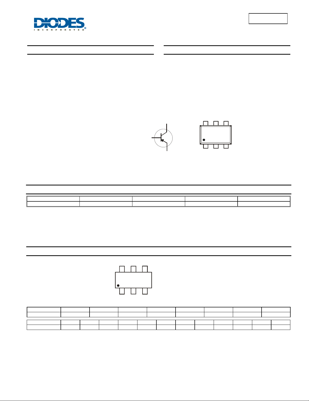
Top View Device Symbol
100V LOW V
Mechanical Data
• Case: SOT-363
• Case Material: Molded Plastic, “Green” Molding Compound.
• Moisture Sensitivity: Level 1 per J-STD-020
• Terminals: Finish - Matte Tin annealed over Alloy 42 leadframe.
• Weight: 0.006 grams (approximate)
C
B
E
PNP SURFACE MOUNT TRANSISTOR
CE(SAT)
UL Flammability Classification Rating 94V-0
Solderable per MIL-STD-202, Method 208
E
B
Top View
Pin Out Configuration
DSS9110Y
Ordering Information (Note 3)
Product Marking Reel size (inches) Tape width (mm) Quantity per reel
DSS9110Y-7 ZP5 7 8mm 3,000
Notes: 1. No purposefully added lead.
2. Diodes Inc’s “Green” Policy can be found on our website at http://www.diodes.com
3. For packaging details, go to our website at http://www.diodes.com
Marking Information
Date Code Key
Year 2010 2011 2012 2013 2014 2015 2016 2017
Code X Y Z A B C D E
Month Jan Feb Mar Apr May Jun Jul Aug Sep Oct Nov Dec
Code 1 2 3 4 5 6 7 8 9 O N D
ZP5
DSS9110Y
Document number: DS31678 Rev. 2 - 2
ZP5 = Product Type Marking Code
YM = Date Code Marking
Y = Year (ex: V = 2008)
YM
M = Month (ex: 9 = September)
1 of 6
www.diodes.com
October 2010
© Diodes Incorporated

θ
P, P
OWER
PATIO
C
O
CTO
R CUR
REN
T
T
R
T
T
HER
R
TANC
Maximum Ratings @T
= 25°C unless otherwise specified
A
Characteristic Symbol Value Unit
Collector-Base Voltage
Collector-Emitter Voltage
Emitter-Base Voltage
V
V
V
Collector Current - Continuous
Peak Pulse Collector Current
I
Base Current – Continuous
Thermal Characteristics
Characteristic Symbol Value Unit
Power Dissipation (Note 4) @ TA = 25°C PD
Thermal Resistance, Junction to Ambient (Note 4) @ TA = 25°C
Operating and Storage Temperature Range
Notes: 4. Device mounted on FR-4 PCB, with minimum recommended pad layout.
0.8
R
T
, T
J
CBO
CEO
EBO
I
C
CM
I
B
10
JA
STG
DSS9110Y
-120 V
-100 V
-5 V
-1 A
-3 A
-0.3 A
625 mW
200
-55 to +150
Pw = 100µs
°C/W
°C
0.6
N (W)
0.4
(A)
1
0.1
DISSI
LLE
RC/W
°
0.2
D
0
050100150200
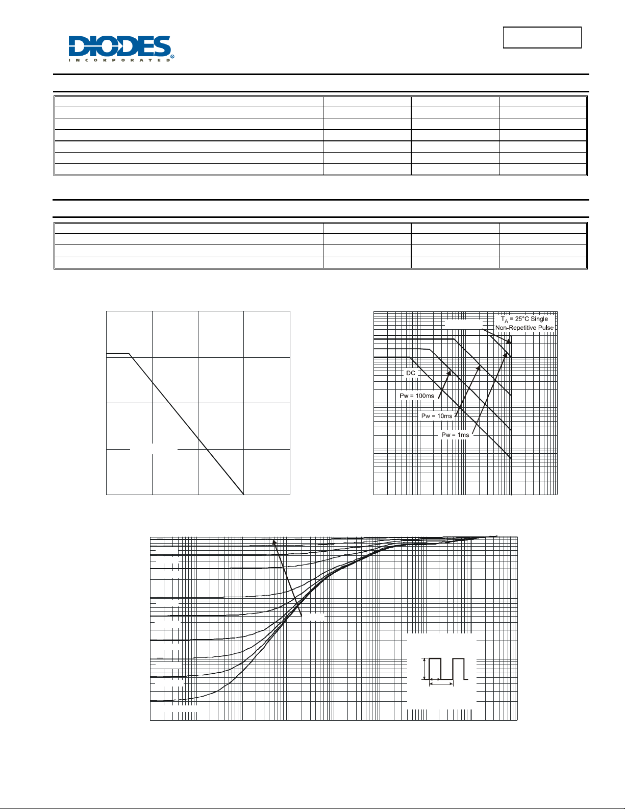
Fig. 1 Power Dissipation vs. Ambient Temperature
= 200
θ
JA
T , AMBIENT TEMPERATURE ( C)
A
°
0.01
C
I,
0.001
0.1 1 10 100 1,000
V , COLLECTOR EMITTER VOLTAGE (V)
CE
Fig. 2 Safe Operating Area
1
D = 0.7
E
D = 0.5
D = 0.3
ESIS
0.1
D = 0.1
MAL
0.01
ANSIEN
r(t),
D = 0.05
D = 0.02
D = 0.01
D = 0.005
D = Single Pulse
D = 0.9
R (t) = r(t) *
θ
JA
R = 163°C/W
JA
P(pk)
t
1
t
2
T - T = P * R (t)
JA JA12θ
Duty Cycle, D = t /t
R
θθJA
0.001
0.00001 0.0001 0.001 0.01 0.1 1 10 100 1,000
t , PULSE DURATION TIME (s)
1
Fig. 3 Transient Therma l R esponse
DSS9110Y
Document number: DS31678 Rev. 2 - 2
2 of 6
www.diodes.com
October 2010
© Diodes Incorporated
 Loading...