

Page 1
Features
• Epitaxial Planar Die Construction
• Ideal for Medium Power Amplification and Switching
• “Lead Free”, RoHS Compliant (Note 1)
• Halogen and Antimony Free. "Green" Device (Note 2)
• Qualified to AEC-Q101 Standards for High Reliability
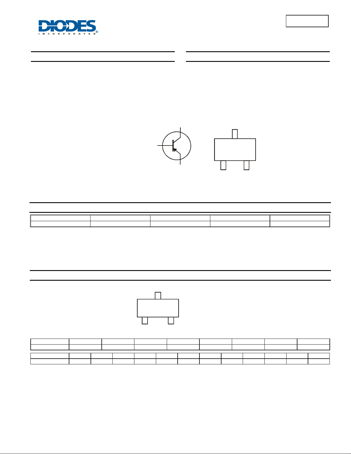
SOT-23
Top View
20V LOW V
PNP SURFACE MOUNT TRANSISTOR
CE(sat)
Mechanical Data
• Case: SOT-23
• Case Material: Molded Plastic, "Green” Molding Compound.
UL Flammability Classification Rating 94V-0
• Moisture Sensitivity: Level 1 per J-STD-020
• Terminals: Finish — Matte Tin annealed over Copper leadframe.
Solderable per MIL-STD-202, Method 208
• Weight: 0.008 grams (approximate)
C
C
B
E
Device Symbol Pin-Out Top
B
DSS5320T
E
Ordering Information (Note 3)
Product Marking Reel size (inches) Tape width (mm) Quantity per reel
DSS5320T-7 ZP4 7 8mm 3,000
Notes: 1. No purposefully added lead.
2. Diodes Inc’s “Green” Policy can be found on our website at http://www.diodes.com
3. For packaging details, go to our website at http://www.diodes.com
Marking Information
Date Code Key
Year 2009 2010 2011 2012 2013 2014 2015 2016
Code W X Y Z A B C D
Month Jan Feb Mar Apr May Jun Jul Aug Sep Oct Nov Dec
Code 1 2 3 4 5 6 7 8 9 O N D
DSS5320T
Document number: DS31620 Rev. 2 - 2
ZP4
www.diodes.com
ZP4 = Product Type Marking Code
YM = Date Code Marking
Y = Year (ex: V = 2008)
YM
M = Month (ex: 9 = September)
1 of 5
October 2010
© Diodes Incorporated
Page 2
θ
P, P
O
R
PATIO
C
O
C
TOR
CUR
REN
T
Maximum Ratings @T
= 25°C unless otherwise specified
A
Characteristic Symbol Value Unit
Collector-Base Voltage
Collector-Emitter Voltage
Emitter-Base Voltage
Peak Pulse Current
Repetitive Peak Pulse Current (Note 4)
Continuous Collector Current
Base Current
V
V
V
I
I
CRP
CBO
CEO
EBO
CM
I
C
I
B
Thermal Characteristics
Characteristic Symbol Value Unit
Power Dissipation (Note 5) @ TA = 25°C PD
Thermal Resistance, Junction to Ambient Air (Note 4) @ TA = 25°C
Operating and Storage Temperature Range
Notes: 4. Operated under pulsed conditions: pulse width ≤100ms, duty cycle ≤ 0.25.
5. Device mounted on 15mm x 15mm x1.6mm FR4 PCB with high coverage of single sided 1oz copper, in still air conditions.
0.8
R
, T
T
J
JA
STG
100
DSS5320T
-20 V
-20 V
-5 V
-5 A
-3 A
-2 A
-0.5 A
600 mW
209 °C/W
-55 to +150 °C
10
0.6
N (W)
(A)
1
0.4
DISSI
0.1
WE
D
0.2
R°C/W
= 209
θ
JA
0
050100150200
T , AMBIENT TEMPERATURE ( C)
A
°
Fig. 1 Power Dissipation vs. Ambient Temperature
LLE
C
I,
0.01
0.001
0.1 1 10 100
V , COLLECTOR EMITTER VOLTAGE (V)
CE
Fig. 2 Safe Operating Area
DSS5320T
Document number: DS31620 Rev. 2 - 2
2 of 5
www.diodes.com
October 2010
© Diodes Incorporated
Page 3

)
)
r
C
O
C
O
R CUR
R
C CUR
R
T
G
DSS5320T
Electrical Characteristics @T
= 25°C unless otherwise specified
A
Characteristic Symbol Min Typ Max Unit Test Conditions
Collector-Base Cutoff Current
Emitter-Base Cutoff Current
Collector-Base Breakdown Voltage
Collector-Emitter Breakdown Voltage (Note 6)
Emitter-Base Breakdown Voltage
DC Current Gain (Note 5)
Collector-Emitter Saturation Voltage (Note 6)
Equivalent On-Resistance
Base-Emitter Saturation Voltage
Base-Emitter Turn-on Voltage
Transition Frequency
Output Capacitance
Turn-On Time
Delay Time
Rise Time
Turn-Off Time
Storage Time
Fall Time
Notes: 6. Measured under pulsed conditions. Pulse width = 300μs. Duty cycle ≤2%.
I
CBO
I
EBO
BV
CBO
BV
CEO
BV
EBO
h
FE
V
CE(sat)
R
CE(sat
V
BE(sat)
V
⎯ ⎯
BE(on
f
T
C
ob
t
on
t
d
t
t
off
t
s
t
f
⎯ ⎯
⎯ ⎯
⎯ ⎯
-20
-20
-5
220
220
200
150
100
⎯ ⎯
⎯ ⎯
⎯ ⎯
⎯ ⎯
⎯ ⎯
⎯ ⎯
⎯ ⎯
⎯ ⎯
⎯ ⎯
⎯ ⎯
⎯ ⎯
⎯ ⎯
⎯ ⎯
⎯ ⎯
⎯ ⎯
⎯ ⎯
100 180
⎯
⎯
⎯
⎯
⎯
⎯
⎯
25 50 pF
67
23
44
224
184
40
-100
-50
-100 nA
-70
-130
-230
-210
-300
105
-1.1 V
-1.2 V
-1.2 V
⎯
⎯
⎯
⎯
⎯
⎯
⎯
nA
μA
= -20V, IE = 0
V
CB
= -20V, IE = 0, TA = 150°C
V
CB
VEB = -5V, IC = 0
V
IC = -100μA
V
IC = -10mA
V
IE = -100μA
V
= -2V, IC = -0.1A
CE
= -2V, IC = -0.5A
V
CE
⎯
mV
mΩ
= -2V, IC = -1A
V
CE
= -2V, IC = -2A
V
CE
= -2V, IC = -3A
V
CE
I
= -0.5A, IB = -50mA
C
= -1A, IB = -50mA
I
C
= -2A, IB = -100mA
I
C
= -2A, IB = -200mA
I
C
= -3A, IB = -300mA
I
C
IE = -2A, IB = -200mA
= -2A, IB = -100mA
I
C
IC = -3A, IB = -300mA
VCE = -2V, IC = -1A
V
= -5V, IC = -100mA,
MHz
CE
f = 100MHz
VCB = -10V, f = 1MHz
ns
ns
ns
V
= -10V, IC = -1A,
CC
ns
= -IB2 = -50mA
I
B1
ns
ns
2.0
1.8
1.6
1.4
ENT (A)
I = 5mA
B
I = 4mA
B
1.2
I = 3mA
1.0
T
0.8
LLE
0.6
C
I,
0.4
B
I = 2mA
B
I = 1mA
B
0.2
0
01 2 3 45
V , COLLECTOR-EMITTER VOLTAGE (V)
Fig. 3 Typical Collector Current vs. Collector-Emitter Voltage
CE
1,000
AIN
EN
900
800
700
600
500
T = 150°C
A
T = 125°C
A
T = 85°C
A
T = 25°C
A
V = -2V
CE
400
300
FE
h, D
T = -55°C
A
200
100
0
0.001 0.01 0.1 1 10
Fig. 4 Typical DC Current G ain vs. Coll ector Current
I , COLLECTOR CURRENT (A)
C
DSS5320T
Document number: DS31620 Rev. 2 - 2
3 of 5
www.diodes.com
October 2010
© Diodes Incorporated
Page 4

C
O
C
TOR
T
TER
C
O
CTO
R
T
TER
2
T
TER TUR
N-O
N VOLTAG
T
TER
TURATIO
OLTAG
DSS5320T
1
I/I = 10
CB
0.1
-EMI
T = 150°C
VOLTAGE ( V)
T = 125°C
LLE
A
0.01
SATURATION
CE(SAT)
V,
0.001
0.001 0.01 0.1 1 10
Fig. 5 Typical Collector-Emitter Saturation Voltage
I , COLLECTOR CURRENT (A)
C
A
T = -55°C
A
T = 85°C
A
T = 25°C
A
vs. Collector Current
1.
E (V)
1.0
V = -2V
CE
1
-EMI
0.1
VOLTAGE (V)
I/I = 20
CB
T = 125°C
A
T = 150°C
A
LLE
T = 25°C
0.01
T = -55°C
SATURATION
CE(SAT)
V,
0.001
0.001 0.01 0.1 1 10
Fig. 6 Typical Collector-Emitter Saturation Voltage
I , COLLECTOR CURRENT (A)
C
A
A
vs. Collect or Current
1.2
I = 10
E (V)
/I
CB
1.0
T = 85°C
A
0.8
T = - 55°C
A
0.6
T = 25°C
A
0.4
T = 85°C
A
T = 125°C
T = 150°C
0.2
A
BE(ON)
V , BASE-EMI
0
0.001 0.01 0.1 1 10
Fig. 7 Typical Base-Emitter Turn-On Voltage
A
I , COLLECTOR CURRENT (A)
C
vs. Collector Current
Package Outline Dimensions
K
J
A
H
F
D
G
N V
0.8
T = -55°C
A
0.6
T = 25°C
0.4
A
T = 150°C
A
T = 125°C
A
T = 85°C
A
SA
0.2
0
0.001 0.01 0.1 1 10
BE(SAT)
V , BASE-EMI
I , COLLECTOR CURRENT (A)
C
Fig. 8 Typical Base-Emitter Saturation Voltage
vs. Collector Current
SOT-23
Dim Min Max Typ
A 0.37 0.51 0.40
C
B
B 1.20 1.40 1.30
C 2.30 2.50 2.40
D 0.89 1.03 0.915
F 0.45 0.60 0.535
G 1.78 2.05 1.83
H 2.80 3.00 2.90
K1
M
J 0.013 0.10 0.05
K 0.903 1.10 1.00
K1 - - 0.400
L
L 0.45 0.61 0.55
M 0.085 0.18 0.11
0° 8° -
α
All Dimensions in mm
DSS5320T
Document number: DS31620 Rev. 2 - 2
4 of 5
www.diodes.com
October 2010
© Diodes Incorporated
Page 5

DSS5320T
Suggested Pad Layout
DIODES INCORPORATED MAKES NO WARRANTY OF ANY KIND, EXPRESS OR IMPLIED, WITH REGARDS TO THIS DOCUMENT,
INCLUDING, BUT NOT LIMITED TO, THE IMPLIED WARRANTIES OF MERCHANTABILITY AND FITNESS FOR A PARTICULAR
PURPOSE (AND THEIR EQUIVALENTS UNDER THE LAWS OF ANY JURISDICTION).
Diodes Incorporated and its subsidiaries reserve the right to make modifications, enhancements, improvements, corrections or other
changes without further notice to this document and any product described herein. Diodes Incorporat ed does not assume an y liabi lity arising
out of the application or use of this document or any product described herein; neither does Diodes Incorporated convey any license under
its patent or trademark rights, nor the rights of others. Any Customer or user of this document or products described herein in such
applications shall assume all risks of such use and will agree to hold Diodes Incorporated and all the companies whose products are
represented on Diodes Incorporated website, harmless against all damages.
Diodes Incorporated does not warrant or accept any liability whatsoever in respect of any products purchased through unauthorized sales
channel. Should Customers purchase or use Diodes Incorporated products for any unintended or unauthorized application, Customers shall
indemnify and hold Diodes Incorporated and its representatives harmless against all claims, damages, expenses, and attorney fees arising
out of, directly or indirectly, any claim of personal injury or death associated with such unintended or unauthorized application.
Products described herein may be covered by one or more United States, international or foreign patents pending. Product names and
markings noted herein may also be covered by one or more United States, international or foreign trademarks.
Diodes Incorporated products are specifically not authorized for use as critical components in life support devices or systems without the
express written approval of the Chief Executive Officer of Diodes Incorporated. As used herein:
A. Life support devices or systems are devices or systems which:
1. are intended to implant into the body, or
2. support or sustain life and whose failure to perform when properly used in accordance with instructions for use provided in
the labeling can be reasonably expected to result in significant injury to the user.
B. A critical component is any component in a life support device or system whose failure to perform can be reasonably expected to cause
the failure of the life support device or to affect its safety or effectiveness.
Customers represent that they have all necessary expertise in the safety and regulatory ramifications of their life support devices or systems,
and acknowledge and agree that they are solely responsible for all legal, regulatory and safety-related requirements concerning their
products and any use of Diodes Incorporated products in such safety-critical, life support devices or systems, notwithstanding any devicesor systems-related information or support that may be provided by Diodes Incorporated. Further, Customers must fully indemnify Diodes
Incorporated and its representatives against any damages arising out of the use of Diodes Incorpor ated products in such safety-critical, life
support devices or systems.
Copyright © 2010, Diodes Incorporated
www.diodes.com
Y
Z
X
E
C
IMPORTANT NOTICE
LIFE SUPPORT
Dimensions Value (in mm)
Z 2.9
X 0.8
Y 0.9
C 2.0
E 1.35
DSS5320T
Document number: DS31620 Rev. 2 - 2
5 of 5
www.diodes.com
October 2010
© Diodes Incorporated
 Loading...