

Page 1
θ
Features
• Epitaxial Planar Die Construction
• Low Collector-Emitter Saturation Voltage, V
• Complementary PNP Type Available (DSS5160U)
• Ultra-Small Surface Mount Package
• Lead Free By Design/RoHS Compliant (Note 1)
• "Green Device" (Note 2)
NEW PRODUCT
Maximum Ratings @T
Collector-Base Voltage
Collector-Emitter Voltage
Emitter-Base Voltage
Collector Current - Continuous
Peak Pulse Collector Current
Base Current (DC)
Peak Base Current
= 25°C unless otherwise specified
A
Characteristic Symbol Value Unit
CE(SAT)
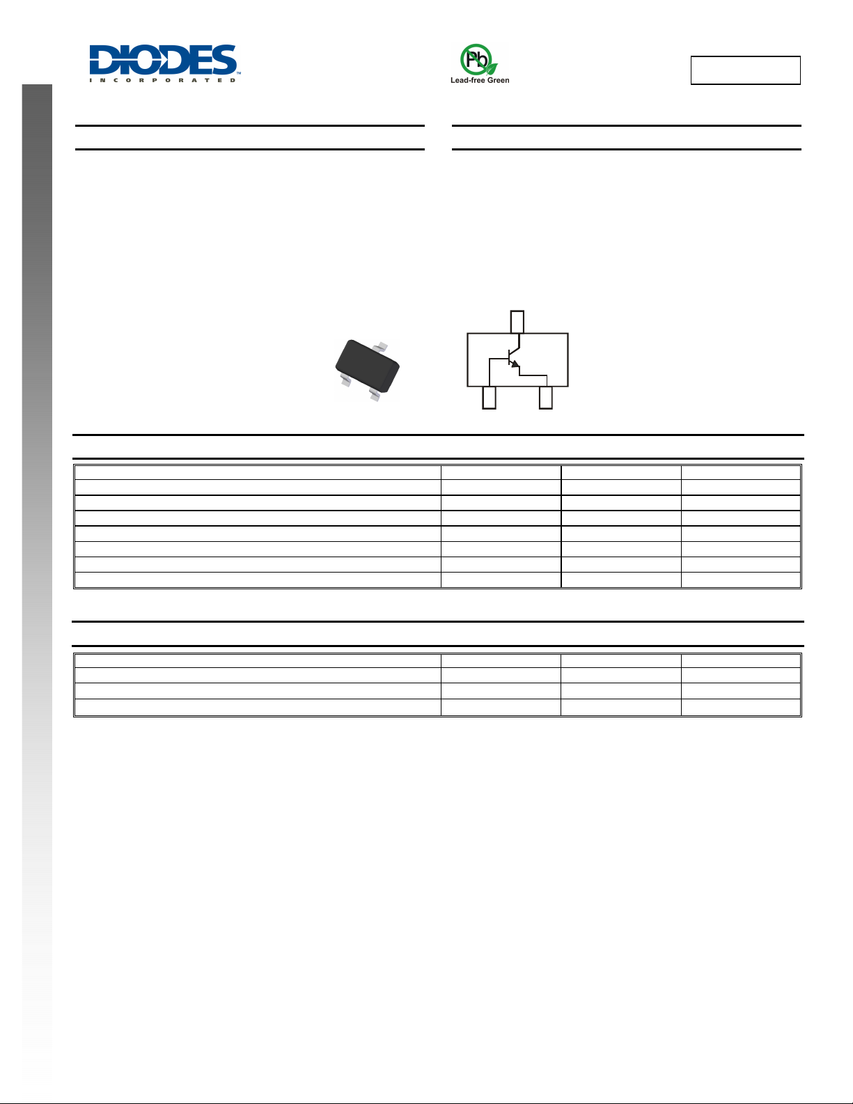
Top View
DSS4160U
LOW V
NPN SURFACE MOUNT TRANSISTOR
CE(SAT)
Mechanical Data
• Case: SOT-323
• Case Material: Molded Plastic, “Green” Molding Compound.
UL Flammability Classification Rating 94V-0
• Moisture Sensitivity: Level 1 per J-STD-020D
• Terminals: Finish ⎯ Matte Tin annealed over Copper Plated
Alloy 42 leadframe. Solderable per MIL-STD-202, Method 208
• Terminal Connections: See Diagram
• Marking Information: See Page 4
• Ordering Information: See Page 4
• Weight: 0.006 grams (approximate)
C
B
Device Schematic
V
CBO
V
CEO
V
EBO
I
C
I
CM
I
B
I
BM
E
80 V
60 V
5 V
1 A
2 A
300 mA
1 A
Thermal Characteristics
Characteristic Symbol Value Unit
Power Dissipation (Note 3) @ TA = 25°C PD
Thermal Resistance, Junction to Ambient (Note 3) @ TA = 25°C
Operating and Storage Temperature Range
Notes: 1. No purposefully added lead.
DSS4160U
Document number: DS31684 Rev. 2 - 2
2. Diode’s Inc.’s “Green” policy can be found on our website at http://www.diodes.com/products/lead_free/index.php.
3. Device mounted on FR-4 PCB with minimum recommended pad layout.
www.diodes.com
1 of 5
R
JA
T
, T
J
STG
400 mW
313
-55 to +150
°C/W
°C
March 2009
© Diodes Incorporated
Page 2
(BR)
(BR)
(BR)
)
)
)
r
P, P
O
R
PAT
O
N
C
O
CTO
R
C
U
R
R
T
Electrical Characteristics @T
= 25°C unless otherwise specified
A
Characteristic Symbol Min Typ Max Unit Test Condition
OFF CHARACTERISTICS
Collector-Base Breakdown Voltage
Collector-Emitter Breakdown Voltage (Note 4)
Emitter-Base Breakdown Voltage
Collector Cutoff Current
V
V
V
I
Collector Cutoff Current
Emitter Cutoff Current
I
ON CHARACTERISTICS (Note 4)
DC Current Gain
Collector-Emitter Saturation Voltage
V
CE(SAT)
NEW PRODUCT
Collector-Emitter Saturation Resistance
Base-Emitter Saturation Voltage
Base-Emitter Turn On Voltage
SMALL SIGNAL CHARACTERISTICS
Output Capacitance
Current Gain-Bandwidth Product
SWITCHING CHARACTERISTICS
Turn-On Time
Delay Time
Rise Time
Turn-Off Time
Storage Time
Fall Time
Notes: 4. Measured under pulsed conditions. Pulse width = 300μs. Duty cycle ≤2%.
600
R
CE(SAT
V
BE(SAT
V
BE(ON
C
80
CBO
I
CES
EBO
CBO
CEO
EBO
60
5
⎯ ⎯
⎯ ⎯
⎯ ⎯
250
h
FE
200
100
⎯ ⎯
⎯
⎯ ⎯
⎯ ⎯
⎯ ⎯
⎯ ⎯
obo
f
T
t
on
t
d
t
t
off
t
⎯
s
t
⎯
f
150
⎯
⎯
⎯
⎯
⎯ ⎯
⎯ ⎯
⎯ ⎯
⎯
⎯
⎯
⎯
⎯
⎯
⎯ ⎯
63
33
30
420
380
40
10
V
IC = 100μA, IE = 0
V
IC = 10mA, IB = 0
V
IE = 100μA, IC = 0
nA
100
50
100 nA
100 nA
⎯
⎯
⎯
115
150
280
280 mΩ
1.1 V
0.9 V
10 pF
⎯
⎯
⎯
⎯
⎯
⎯
VCB = 60V, IE = 0
μA
V
VCE = 60V, VBE = 0
V
V
V
⎯
V
I
mV
I
I
IC = 1A, IB = 100mA
IC = 1A, IB = 50mA
V
VCB = 10V, f = 1.0MHz
MHz
VCE = 10V, IC = 50mA, f = 100MHz
ns
ns
ns
V
ns
I
ns
ns
DSS4160U
= 60V, IE = 0, TA = 150°C
CB
= 5V, IC = 0
EB
= 5V, IC = 1mA
CE
= 5V, IC = 500mA
CE
= 5V, IC = 1A
CE
= 100mA, IB = 1mA
C
= 500mA, IB = 50mA
C
= 1A, IB = 100mA
C
= 5V, IC = 1A
CE
= 10V
CC
= 0.5A, IB1 = IB2 = 25mA
C
Pw = 1ms
Pw = 10ms
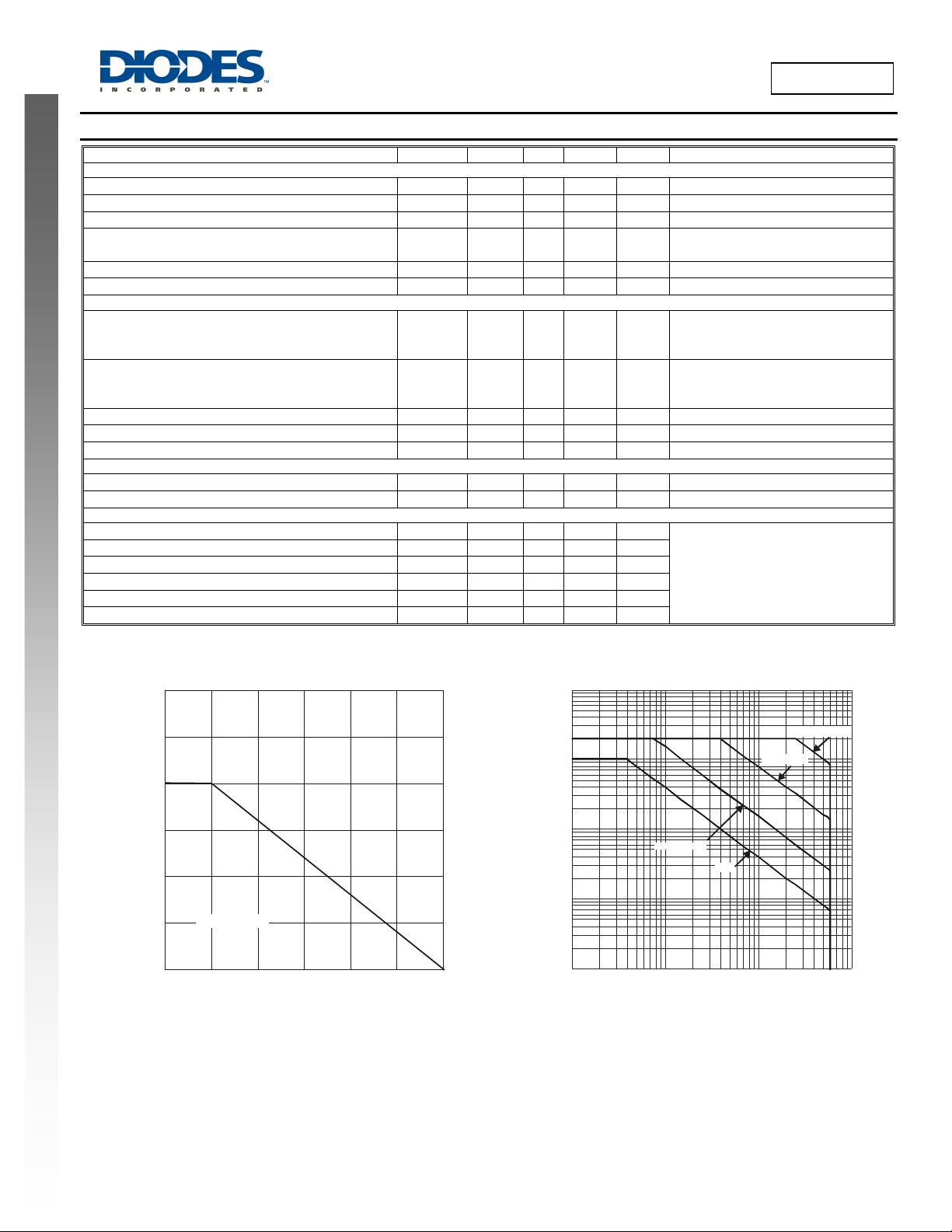
(mW)
I
DISSI
WE
D
500
400
300
200
100
0
0
R = 313°C/W
θ
JA
25 50
T , AMBIENT TEMPERATURE (°C)
A
75 100 125
Fig. 1 Power Dissipation vs.
Ambient Temperature (Note 3)
150
(A)
1
EN
0.1
Pw = 100ms
DC
LLE
0.01
C
I,
0.001
0.1 1 10 100
V , COLLECTOR-EMITTER VOLTAGE (V)
CE
Fig. 2 Typical Collector Current
vs. Collector-Emitter Voltage (Note 3)
DSS4160U
Document number: DS31684 Rev. 2 - 2
2 of 5
www.diodes.com
March 2009
© Diodes Incorporated
Page 3

C CUR
REN
T
G
N
C
O
CTO
R
T
T
R
T
TER TUR
N-O
N VOLTAG
T
TER
TURATIO
N VOLTAG
CAPACIT
N
C
NEW PRODUCT
DSS4160U
E
-EMI
VOLTAGE (V)
LLE
0.01
SATURATION
CE(SAT)
V,
0.001
1.2
E (V)
1.0
1
I/I = 10
CB
0.1
T = 150°C
A
T = 85°C
A
T = 25°C
A
T = -55°C
A
0.1 1,000
1 10 100 10,000
I , COLLECTOR CURRENT (mA)
Fig. 4 Typical Collector-Emitter Saturation Voltage
C
vs. Collector Current
I = 10
/I
CB
1,000
T = 150°C
800
A
AI
600
T = 85°C
A
400
FE
h, D
200
T = 25°C
A
T = -55°C
A
0
1 10 100 10,000
I , COLLECTOR CURRENT (mA)
Fig. 3 Typical DC Current Gain vs. Collector Current
C
1,000
1.2
E (V)
V = 5V
CE
1.0
V = 5V
CE
0.8
T = -55°C
A
0.6
T = 25°C
A
0.4
T = 85°C
A
0.2
T = 150°C
A
BE(ON)
0
V , BASE-EMI
0.1 10 100 1,000 10,000
1
I , COLLECTOR CURRENT (mA)
C
Fig. 5 Typical Base-Emitter Turn-On Voltage
vs. Collector Current
180
150
f = 1MHz
120
E (pF)
A
90
C
ibo
60
0.8
T = -55°C
A
0.6
T = 25°C
SA
0.4
0.2
A
T = 85°C
A
T = 150°C
A
0
0.1 10 100 10,000
BE(SAT)
V , BASE-EMI
11,000
I , COLLECTOR CURRENT (mA)
C
Fig. 6 Typical Base-Emitter Saturation Voltage
vs. Collector Current
30
C
0
obo
0.1 1 10 100
V , REVERSE VOLTAGE (V)
R
Fig. 7 Typical Capacitance Characteristics
DSS4160U
Document number: DS31684 Rev. 2 - 2
3 of 5
www.diodes.com
March 2009
© Diodes Incorporated
Page 4

T
R
T
T
HER
R
TANC
1
D = 0.7
D = 0.5
D = 0.3
0.1
D = 0.1
0.01
D = 0.05
D = 0.02
D = 0.01
D = 0.005
D = Single Pulse
D = 0.9
0.00001 0.0001 0.001 0.01 0.1 1 10 100
t , PULSE DURATION TIME (s)
1
NEW PRODUCT
E
ESIS
MAL
ANSIEN
r(t),
0.001
Fig. 8 Transient Thermal Response (Note 3)
Ordering Information (Note 5)
Part Number Case Packaging
DSS4160U-7 SOT-323 3000/Tape & Reel
Notes: 5. For packaging details, go to our website at http://www.diodes.com/datasheets/ap02007.pdf.
R (t) = r(t) *
θ
JA
R = 310°C/W
JA
P(pk)
t
1
t
2
T - T = P * R (t)
JA JA12θ
Duty Cycle, D = t /t
DSS4160U
R
θθJA
10,0001,000
Marking Information
ZN9
Date Code Key
Year 2008 2009 2010 2011 2012 2013 2014 2015
Code V W X Y Z A B C
Month Jan Feb Mar Apr May Jun Jul Aug Sep Oct Nov Dec
Code 1 2 3 4 5 6 7 8 9 O N D
ZN9 = Product Type Marking Code
YM = Date Code Marking
Y = Year (ex: V = 2008)
YM
M = Month (ex: 9 = September)
Package Outline Dimensions
K
J
DSS4160U
Document number: DS31684 Rev. 2 - 2
A
SOT-323
Dim Min Max Typ
C
B
A 0.25 0.40 0.30
B 1.15 1.35 1.30
C 2.00 2.20 2.10
G
H
M
D - - 0.65
G 1.20 1.40 1.30
H 1.80 2.20 2.15
J 0.0 0.10 0.05
K 0.90 1.00 1.00
L 0.25 0.40 0.30
D
L
M 0.10 0.18 0.11
0° 8° -
α
All Dimensions in mm
4 of 5
www.diodes.com
March 2009
© Diodes Incorporated
Page 5

DSS4160U
Suggested Pad Layout
NEW PRODUCT
Diodes Incorporated and its subsidiaries reserve the right to make modifications, enhancements, improvements, corrections or other changes
without further notice to any product herein. Diodes Incorporated does not assume any liability arising out of the application or use of any product
described herein; neither does it convey any license under its patent rights, nor the rights of others. The user of products in such applications shall
assume all risks of such use and will agree to hold Diodes Incorporated and all the companies whose products are represented on our website,
harmless against all damages.
Diodes Incorporated products are not authorized for use as critical components in life support devices or systems without the expressed written
approval of the President of Diodes Incorporated.
Y
Z
X
E
C
IMPORTANT NOTICE
LIFE SUPPORT
Dimensions Value (in mm)
Z 2.8
X 0.7
Y 0.9
C 1.9
E 1.0
DSS4160U
Document number: DS31684 Rev. 2 - 2
5 of 5
www.diodes.com
March 2009
© Diodes Incorporated
 Loading...