

Diodes DRTR5V0U2SR User Manual
Features
IEC 61000-4-2 (ESD): Air ±15kV, Contact ±8kV
2 Channels of ESD Protection
Low Channel Input Capacitance of 1.0pF Typical
Typically Used at High Speed Ports such as USB 2.0,
IEEE1394, Serial ATA, DVI, HDMI, PCI
Totally Lead-Free & Fully RoHS Compliant (Notes 1 & 2)
Halogen and Antimony Free. “Green” Device (Note 3)
Qualified to AEC-Q101 Standards for High Reliability
NEW PRODUCT
2 CHANNEL LOW CAPACITANCE TVS DIODE ARRAY
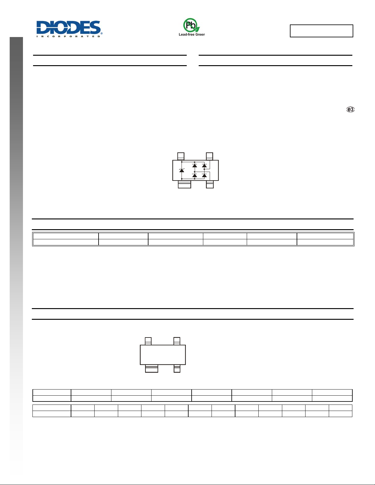
Mechanical Data
Case: SOT143
Case Material: Molded Plastic, “Green” Molding Compound. UL
Flammability Classification Rating 94V-0
Moisture Sensitivity: Level 1 per J-STD-020
Terminals: Matte Tin Finish annealed over Alloy 42 leadframe
(Lead Free Plating). Solderable per MIL-STD-202, Method 208
Weight: 0.009 grams (approximate)
V
CC
12
GND
Device Schematic
I/O2
34
I/O1
DRTR5V0U2SR
Ordering Information (Note 4)
Product Compliance Marking Reel size (inches) Tape width (mm) Quantity per reel
DRTR5V0U2SR-7 AEC-Q101 TE9 7 8 3,000/Tape & Reel
Notes: 1. No purposely added lead. Fully EU Directive 2002/95/EC (RoHS) & 2011/65/EU (RoHS 2) compliant.
2. See http://www.diodes.com/quality/lead_free.html for more information about Diodes Incorporated’s definitions of Halogen- and Antimony-free, "Green"
and Lead-free.
3. Halogen- and Antimony-free "Green” products are defined as those which contain <900ppm bromine, <900ppm chlorine (<1500ppm total Br + Cl) and
<1000ppm antimony compounds.
4. For packaging details, go to our website at http://www.diodes.com/products/packages.html.
Marking Information
Date Code Key
Year 2013 2014 2015 2016 2017 2018 2019
Code A B C D E F G
Month Jan Feb Mar Apr May Jun Jul Aug Sep Oct Nov Dec
Code 1 2 3 4 5 6 7 8 9 O N D
TE9
TV2
YM
TE9 = Product Type Marking Code
YM = Date Code Marking
Y = Year (ex: A = 2013)
M = Month (ex: 9 = September)
DRTR5V0U2SR
Document number: DS36005 Rev. 3 - 2
1 of 4
www.diodes.com
August 2013
© Diodes Incorporated
P
P
O
R
PATIO
N
P
P
U
RATIN
G
O
F
DRTR5V0U2SR
Maximum Ratings (@T
= +25°C, unless otherwise specified)
A
Characteristic Symbol Value Unit Conditions
Peak Pulse Current
ESD Protection – Contact Discharge
ESD Protection – Air Discharge
I
PP
V
ESD_Contact
V
ESD_Air
5 A 8/20µs, Per Figure 3
±8 kV Standard IEC 61000-4-2
±15 kV Standard IEC 61000-4-2
Thermal Characteristics
Characteristic Symbol Value Unit
Power Dissipation (Note 5)
Thermal Resistance, Junction to Ambient (Note 5)
Operating and Storage Temperature Range
NEW PRODUCT
P
D
R
θJA
, T
T
J
STG
Electrical Characteristics (@T
= +25°C, unless otherwise specified.)
A
Characteristic Symbol Min Typ Max Unit Test Conditions
Reverse Standoff Voltage
Channel Leakage Current (Note 6, 7)
Reverse breakdown voltage
Forward Voltage (Note 7)
Dynamic Resistance (Note 7)
I/O to GND Capacitance (Note 7)
Notes: 5. Device mounted on FR-4 PCB pad layout (2oz copper) as shown on Diodes, Inc. suggested pad layout AP02001, which can be found on our website at
http://www.diodes.com.
6. Short duration pulse test used to minimize self-heating effect.
7. Measured from pin 2 or pin 3 to GND.
8. For information on the impact of Diodes' USB 2.0 compatible ESD protectors on signal integrity including eye diagram plots, please refer to AN77 at the
following URL: http://www.diodes.com/destools/appnote_dnote.html.
V
RWM
V
V
R
C
(I/O-GND)
I
R
BR
F
DYN
— — 5.5 V —
— 1 100 nA
6.0 — 9.0 V
— 0.8 — V
— 0.9 —
— 1.0 1.5 pF
400
100
400 mW
310 °C/W
-65 to +150 °C
VR = 3V
IR = 1mA, from pin 4 to pin 1
IF = 8mA
Ω
IPP = 1A, tp = 8/20μs
V
(I/O-GND)
= 0V, f = 1MHz
Note 5
75
%
(mW)
350
300
250
200
50
DISSI
WE
,
D
150
100
LSE DE
EAK
25
PEAK POWER OR CURRENT
50
0
0
25 50
T , AMBIENT TEMPERATURE (°C)
A
75 100 125
150
Figure 1 Power Dissipation vs. Ambient Temperature
0
0
25 50
T , AMBIENT TEMPERATURE (°C)
A
75 100 125
Figure 2 Pulse Derating Curve
150
175 200
DRTR5V0U2SR
Document number: DS36005 Rev. 3 - 2
2 of 4
www.diodes.com
August 2013
© Diodes Incorporated
 Loading...