

Page 1
Please click here to visit our online spice models database.
Features
• Epitaxial Planar Die Construction
• One Transistor and One Sw
• Lead Free By
• "Green" Dev
Design/RoHS Compliant (Note 1)
ice (Note 2)
itching Diode in One Package
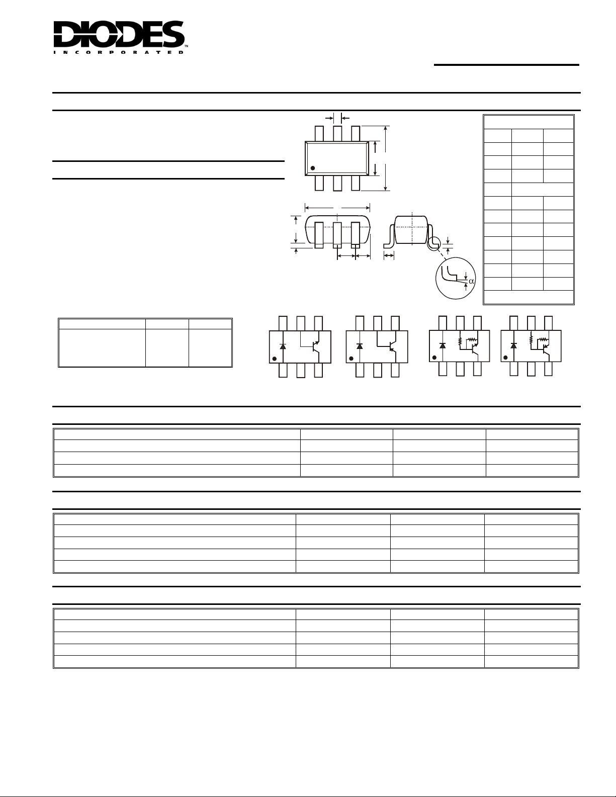
Mechanical Data
• Case: SOT-363
• Case Material: Molded Plastic. "Green" Molding
Compound. UL Flammability
• Moisture Sensitivity
• Terminal Connections: See Diagram
• Terminals: Finish - Matte Tin annealed over Alloy
leadframe. Solderable per MIL-STD-202, Method 208
• Marking Information: See Page 8
• Ordering Information: See Page 8
• Weight: 0.008 grams (approximate)
P/N R1 (NOM) R2 (NOM)
DRDNB16W
DRDPB16W
DRDNB26W
DRDPB26W
: Level 1 per J-STD-020D
Classification Rating 94V-0
1K
1K
220
220
10K
10K
4.7K
4.7K
42
K
J
DRDN010W/
DRDN005W
A
H
D
DRD (xxxx) W
COMPLEX ARRAY FOR RELAY DRIVERS
B C
L
F
DRDP006W
M
R2
R1
DRDNB16W/
DRDNB26W
SOT-363
Dim Min Max
A 0.10 0.30
B 1.15 1.35
C 2.00 2.20
D 0.65 Nominal
F 0.30 0.40
H 1.80 2.20
J
K 0.90 1.00
L 0.25 0.40
M 0.10 0.25
α
All Dimensions in mm
DRDPB16W/
DRDPB26W
R1
⎯
0°
0.10
8°
R2
Maximum Ratings, Total Device @T
Characteristic Symbol Value Unit
Power Dissipation (Note 3)
Thermal Resistance, Junction to Ambient Air (Note 3)
Operating and Storage Temperature Range
Maximum Ratings, DRDN010W NPN Transistor @T
Characteristic Symbol Value Unit
Collector-Base Voltage
Collector-Emitter Voltage
Emitter-Base Voltage
Collector Current (Note 3)
Maximum Ratings, DRDN005W NPN Transistor @T
Characteristic Symbol Value Unit
Collector-Base Voltage
Collector-Emitter Voltage
Emitter-Base Voltage
Collector Current – Continuous (Note 3)
Notes: 1. No purposefully added lead.
DS30573 Rev. 10 - 2
2. Diodes Inc.'s "Green" policy can be found on our website at http://www.diodes.com/products/lead_free/index.php.
3. Device mounted on FR-4 PCB, 1 inch x 0.85 inch x 0.062 inch; pad layout as shown on Diodes Inc. suggested pad layout document AP02001, which
can be found on page 9 or our website at http://www.diodes.com/datasheets/ap02001.pdf.
= 25°C unless otherwise specified
A
P
D
R
JA
θ
TJ, T
STG
= 25°C unless otherwise specified
A
V
CBO
V
CEO
V
EBO
I
C
= 25°C unless otherwise specified
A
V
CBO
V
CEO
V
EBO
I
C
1 of 9
www.
diodes.com
200 mW
625
-55 to +150
45 V
18 V
5 V
1000 mA
80 V
80 V
4.0 V
500 mA
°C/W
°C
DRD (xxxx) W
© Diodes Incorporated
Page 2
Maximum Ratings, DRDP006W PNP Transistor @T
= 25°C unless otherwise specified
A
Characteristic Symbol Value Unit
Collector-Base Voltage
Collector-Emitter Voltage
Emitter-Base Voltage
Collector Current (Note 3)
V
V
V
CBO
CEO
EBO
I
C
Maximum Ratings, DRDNB16W Pre-Biased NPN Transistor @T
Characteristic Symbol Value Unit
Supply Voltage
Input Voltage
Output Current
V
CC
V
IN
I
C
Maximum Ratings, DRDNB26W Pre-Biased NPN Transistor @T
Characteristic Symbol Value Unit
Supply Voltage
Input Voltage
Output Current
V
CC
V
IN
I
C
Maximum Ratings, DRDPB16W Pre-Biased PNP Transistor @T
Characteristic Symbol Value Unit
Supply Voltage
Input Voltage
Output Current
V
CC
V
IN
I
C
-60 V
-60 V
-5.0 V
-600 mA
= 25°C unless otherwise specified
A
50 V
-5 to +10 V
600 mA
= 25°C unless otherwise specified
A
50 V
-5 to +5 V
600 mA
= 25°C unless otherwise specified
A
-50 V
+5 to -10 V
600 mA
Maximum Ratings, DRDPB26W Pre-Biased PNP Transistor @T
Characteristic Symbol Value Unit
Supply Voltage
Input Voltage
Output Current
Maximum Ratings, Switching Diode @T
= 25°C unless otherwise specified
A
V
CC
V
IN
I
C
Characteristic Symbol Value Unit
Non-Repetitive Peak Reverse Voltage
Peak Repetitive Reverse Voltage
Working Peak Reverse Voltage
DC Blocking Voltage
RMS Reverse Voltage
Forward Continuous Current (Note 3)
Average Rectified Output Current (Note 3)
Non-Repetitive Peak Forward Surge Current @ t = 1.0μs
@ t = 1.0s
DS30573 Rev. 10 - 2
www.diodes.com
2 of 9
V
V
V
V
R(RMS)
I
RM
RRM
RWM
V
I
FM
I
O
FSM
R
= 25°C unless otherwise specified
A
-50 V
+5 to -5 V
-600 mA
100 V
75 V
53 V
500 mA
250 mA
4.0
2.0
© Diodes Incorporated
A
DRD (xxxx) W
Page 3
Electrical Characteristics, DRDN010W NPN Transistor @T
Characteristic Symbol Min Max Unit Test Condition
DC Current Gain
Collector-Emitter Saturation Voltage
Collector-Base Breakdown Voltage
Collector-Emitter Breakdown Voltage
Emitter-Base Breakdown Voltage
Collector Cutoff Current
Emitter Cutoff Current
Current Gain-Bandwidth Product
Capacitance
h
V
CE(SAT)
V
(BR)CBO
V
(BR)CEO
V
(BR)EBO
I
CBO
I
EBO
f
C
FE
obo
T
150 800
⎯
45
18
5
⎯
⎯
100
⎯
0.5 V
⎯
⎯
⎯
1
1
⎯
8 pF
Electrical Characteristics, DRDN005W NPN Transistor @T
Characteristic Symbol Min Max Unit Test Condition
Collector-Base Breakdown Voltage
Collector-Emitter Breakdown Voltage
Emitter-Base Breakdown Voltage
Collector Cutoff Current
Collector Cutoff Current
DC Current Gain
Collector-Emitter Saturation Voltage
Base-Emitter Saturation Voltage
Current Gain-Bandwidth Product
V
(BR)CBO
V
(BR)CEO
V
(BR)EBO
I
CBO
I
CES
h
V
CE(SAT)
V
BE(SAT)
f
FE
T
80
80
4.0
⎯
⎯
100
⎯
⎯
100
= 25°C unless otherwise specified
A
⎯
IC = 100mA, V
CE
= 1V
IC = 300mA, IB = 30mA
V
I
= 100μA, IE = 0
C
V
I
= 1mA, IB = 0
C
V
I
= 100μA, IC = 0
E
μA
V
= 40V, IE = 0
CB
μA
V
= 4V, IC = 0
EB
MHz
VCE = 10V, IC = 50mA, f = 100MHz
VCB = 10V, IE = 0, f = 1MHz
= 25°C unless otherwise specified
A
⎯
⎯
⎯
100 nA
100 nA
⎯ ⎯
0.25 V
1.2 V
⎯
V
V
V
MHz
IC = 100μA, IE = 0
IC = 1.0mA, IB = 0
IE = 100μA, IC = 0
VCB = 60V, IE = 0
VCB = 80V, IE = 0
V
= 60V, IBO = 0V
CE
V
= 80V, IBO = 0V
CE
IC = 10mA, VCE = 1.0V
IC = 100mA, V
IC = 100mA, IB = 10mA
IC = 100mA, VCE = 1.0V
VCE = 2.0V, IC = 10mA,
f = 100MHz
CE
= 1.0V
Electrical Characteristics, DRDP006W PNP Transistor @T
= 25°C unless otherwise specified
A
Characteristic Symbol Min Max Unit Test Condition
DC Current Gain
Collector-Emitter Saturation Voltage
Collector-Base Breakdown Voltage
Collector-Emitter Breakdown Voltage
Emitter-Base Breakdown Voltage
Collector Cutoff Current
Current Gain-Bandwidth Product
Capacitance
h
V
CE(SAT)
V
(BR)CBO
V
(BR)CEO
V
(BR)EBO
I
CBO
C
FE
f
obo
T
100 300
-0.4 V
⎯
-60
-60
-5
⎯
200
⎯
⎯
⎯
⎯
-10 nA
⎯
8 pF
⎯
IC = -150mA, V
IC = -150mA, IB = -15mA
V
I
= -10μA, IE = 0
C
V
I
= -10mA, IB = 0
C
V
I
= -10μA, IC = 0
E
V
= -50V, IE = 0
CB
MHz
VCE = -20V, IC = -50mA, f = 100MHz
VCB = -10V, IE = 0, f = 1MHz
Electrical Characteristics, DRDNB16W Pre-Biased NPN Transistor @T
Characteristic Symbol Min Typ Max Unit Test Condition
Input Voltage
Output Voltage
Input Current
Output Current
DC Current Gain
Gain-Bandwidth Product
DS30573 Rev. 10 - 2
V
V
V
I
O(off)
l(off)
l(on)
O(on)
I
l
G
l
f
T
0.3
3 of 9
www.diodes.com
⎯ ⎯
⎯ ⎯
⎯ ⎯
⎯ ⎯
⎯ ⎯
56
⎯
⎯ ⎯ ⎯
200
0.3V V
V
2.0 V
7.2 mA
0.5
μA
MHz
⎯
VCC = 5V, IO = 100μA
VO = 0.3V, IO = 20mA
IO/Il = 50mA/2.5mA
VI = 5V
VCC = 50V, VI = 0V
VO = 5V, IO = 50mA
VCE = 10V, IE = 5mA, f = 100MHz
= -10V
CE
= 25°C unless otherwise specified
A
DRD (xxxx) W
© Diodes Incorporated
Page 4

Electrical Characteristics, DRDNB26W Pre-Biased NPN Transistor @T
Characteristic Symbol Min Typ Max Unit Test Condition
Input Voltage
Output Voltage
Input Current
Output Current
DC Current Gain
Gain-Bandwidth Product
V
V
V
I
O(off)
l(off)
l(on)
O(on)
I
l
G
l
f
T
0.5
⎯ ⎯
⎯ ⎯
⎯ ⎯
⎯ ⎯
47
200
⎯
⎯ ⎯
0.3V V
⎯ ⎯ ⎯
3.0 V
28 mA
0.5
μA
MHz
⎯
V
VCC = 5V, IO = 100μA
VO = 0.3V, IO = 20mA
IO/Il = 50mA/2.5mA
VI = 5V
VCC = 50V, VI = 0V
VO = 5V, IO = 50mA
VCE = 10V, IE = 5mA, f = 100MHz
Electrical Characteristics, DRDPB16W Pre-Biased PNP Transistor @T
Characteristic Symbol Min Typ Max Unit Test Condition
Input Voltage
Output Voltage
Input Current
Output Current
DC Current Gain
Gain-Bandwidth Product
V
V
V
I
O(off)
l(off)
l(on)
O(on)
I
l
G
l
f
T
-0.3
⎯ ⎯
⎯ ⎯
⎯ ⎯
⎯ ⎯
56
⎯
⎯ ⎯
-2.0 V
-0.3V V
-7.2 mA
-0.5
⎯ ⎯ ⎯
200
⎯
V
VCC = -5V, IO = -100μA
VO = -0.3V, IO = -20mA
IO/Il = -50mA/-2.5mA
VI = -5V
μA
VCC = -50V, VI = 0V
VO = -5V, IO = -50mA
MHz
VCE = -10V, IE = -5mA, f = 100MHz
Electrical Characteristics, DRDPB26W Pre-Biased PNP Transistor @T
Characteristic Symbol Min Typ Max Unit Test Condition
Input Voltage
Output Voltage
Input Current
Output Current
DC Current Gain
Gain-Bandwidth Product
V
V
V
I
O(off)
l(off)
l(on)
O(on)
I
l
G
l
f
T
-0.5
⎯ ⎯
⎯ ⎯
⎯ ⎯
⎯ ⎯
47
⎯
⎯ ⎯
-3.0 V
-0.3V V
-0.5
⎯ ⎯ ⎯
200
V
-28 mA
μA
MHz
⎯
VCC = -5V, IO = -100μA
VO = -0.3V, IO = -20mA
IO/Il = -50mA/-2.5mA
VI = -5V
VCC = -50V, VI = 0V
VO = -5V, IO = -50mA
VCE = -10V, IE = -5mA, f = 100MHz
= 25°C unless otherwise specified
A
= 25°C unless otherwise specified
A
= 25°C unless otherwise specified
A
Electrical Characteristics, Switching Diode @T
Characteristic Symbol Min Max Unit Test Condition
Reverse Breakdown Voltage (Note 4)
V
Forward Voltage
Reverse Current (Note 4)
Total Capacitance
Reverse Recovery Time
Notes: 4. Short duration pulse test used to minimize self-heating effect.
DS30573 Rev. 10 - 2
4 of 9
www.diodes.com
= 25°C unless otherwise specified
A
(BR)R
V
F
75
0.62
⎯
⎯
⎯
⎯ ⎯
0.72
0.855
1.0
1.25
2.5
I
R
⎯
50
30
25
C
T
t
rr
⎯
⎯
4.0 pF
4.0 ns
IR = 10μA
IF = 5.0mA
IF = 10mA
V
IF = 100mA
IF = 150mA
VR = 75V
μA
VR = 75V, TJ = 150°C
μA
μA
VR = 25V, TJ = 150°C
nA
VR = 20V
VR = 0, f = 1.0MHz
IF = IR = 10mA,
I
= 0.1 x IR, RL = 100Ω
rr
DRD (xxxx) W
© Diodes Incorporated
Page 5

P, P
O
R
PAT
O
D
C CUR
R
N
T GAIN
C, OUTPU
T CAPACITANC
F
C
O
CTO
R
T
TER
C
O
CTO
R
T
T
R VO
TAG
Device Characteristics
250
1,000
N (mW)
I
DISSI
WE
D
)
E (p
200
150
100
100
10
R = 625°C/W
50
0
0
40
T , AMBIENT TEMPERATURE (°C)
A
80 120 160
Fig. 1, Power Derating Curve (Total Device)
θ
JA
E
100
FE
h,
V = 1.0V
CE
200
1
0.0001 0.001 0.01 1 100.1
I , COLLECTOR CURRENT (A)
C
Fig. 2, Typical DC Current G ain
vs. Collector Current (DRDN010W)
1,000
f = 1MHz
-EMI
100
LLE
10
SATURATION VOLTAGE (mV)
OBO
1
0.1
V , COLLECTOR-BASE VOLTAGE (V)
CB
1
10
100
Fig. 3, Typical Output Capacitance vs.
Collector-Base Voltage (DRDN010W)
10
1
CE (SAT)
V,
1
0.0001
0.001
I , COLLECTOR CURRENT (A)
C
0.01 0.1
1
10
Fig. 4, Typical Collector Saturation Voltage vs.
Collector Current (DRDN01 0W)
2.0
1.8
E (V)
I = 30mA
1.6
L
C
1.4
I = 10mA
E
1.2
1.0
EMI
I = 1mA
C
C
0.8
0.1
CBO
I , COLLECTOR-BASE CURRENT (nA)
0.01
25 50 75 100 125
T , AMBIENT TEMPERA TURE (ºC)
A
Fig. 5, Typical Collector-Cutoff Current
vs. Ambient T emperature (DRDN005W)
DS30573 Rev. 10 - 2
5 of 9
www.diodes.com
0.6
LLE
0.4
CE
V,
0.2
0
0.001 0.01
0.1
I BASE CURRENT (mA)
B,
Fig. 6, Typical Collector Saturation Region
1
I = 100mA
C
10 100
(DRDN005W)
DRD (xxxx) W
© Diodes Incorporated
Page 6

C
O
C
T
O
R-EMIT
TER
C CUR
R
T
G
T
TER O
OLTAG
GAIN
N
T
H PRODUCT
H
O
O
R
R
C
O
CTO
R
T
T
R VOLT
G
0.500
I
C
0.450
= 10
I
B
0.400
0.350
0.300
T = 25°C
A
0.250
LLE
0.200
T = 150°C
A
10,000
1,000
AIN
EN
100
V = 5V
CE
T = -50°C
A
T = 25°C
A
T = 150°C
A
SATURATION VOLTAGE ( V)
CE(SAT)
V,
E (V)
N V
0.150
0.100
0.050
0
110
I , COLLECTOR CURRENT (mA)
C
Fig. 7, Typical Collector-Emitter Saturation Voltage
vs. Collector Current (DRDN005W)
1.0
V = 5V
0.9
CE
0.8
T = -50°C
A
0.7
0.6
T = 25°C
T = -50°C
A
100
1,000
A
FE
h, D
1,000
z)
(M
10
100
1
1
10 1,000
I , COLLECTOR CURRENT (mA)
C
100
Fig. 8, Typical DC Current Gain vs.
Collector Current (DRDN005W)
0.5
0.4
T = 150°C
A
DWID
10
BA
0.3
BE(ON)
0.2
V , BASE-EMI
0.1
0.1
110
I , COLLECTOR CURRENT (mA)
C
100
Fig. 9, Typical Base-Emitter On Voltage
vs. Collector Current (DRDN005W)
0.6
I
C
= 10
I
B
0.5
0.4
-EMITTE
0.3
T = 150°C
A
LLECT
0.2
SATURATION VOLTAGE (V)
CE(SAT)
0.1
V, C
T = 25°C
A
T = -50°C
A
0
110
I , COLLECTOR CURRENT (mA)
C
100
1,000
Fig.11, Typical Collector-Emitter Saturation Voltage vs.
Collector Current (DRDP006W)
DS30573 Rev. 10 - 2
www.
6 of 9
diodes.com
T
f,
1
1
I , COLLECTOR CURRENT (mA)
C
Fig. 10, Typical Gain Bandwidth P roduct vs.
Collector Curren t (DRDN005W )
1.6
I = 100mA
C
I = 300mA
C
1.4
E (V)
A
1.2
I = 1mA
C
1.0
E
I = 10mA
C
I = 30mA
C
0.8
-EMI
0.6
0.4
LLE
0.2
CE
V,
0
0.001
0.01
0.1 1
I , BASE CURRENT (mA)
B
10 100
Fig. 12, Typical Collec to r Saturation Region (DRDP00 6W)
© Diodes Incorporated
10
DRD (xxxx) W
Page 7

C CUR
R
T
G
MIT
T
R
O
N VOLTAG
GAIN
N
T
H PRODUCT
H
C, CAPACITAN
C
p
F
NST
N
T
NEO
US F
O
R
R
D CUR
REN
T
T
T
O
US R
R
C
U
R
RENT
1,000
V = 5V
CE
T = 150°C
A
AIN
100
EN
FE
h, D
10
T = 25°C
A
T = -50°C
A
1
110100
I , COLLECTOR CURRENT (mA)
C
1,000
Fig. 13, Typical DC Current Gain vs.
Collector Current (DRDP006W)
1,000
V = 5V
z)
CE
(M
100
1.0
V = 5V
0.9
E (V)
0.8
0.7
E
0.6
CE
T = -50°C
A
0.5
0.4
BE(ON)
0.3
V , BASE-E
0.2
0.1
1
I , COLLECTOR CURRENT (mA)
C
10
100
Fig. 14, Typical Base-Emitter On Voltage
vs. Collector Current (DRDP006W)
30
20
)
f = 1MHz
C
ibo
E (
10
1,000
(mA)
WA
A
A
DWID
10
BA
T
f,
1
110
I , COLLECTOR CURRENT (mA)
C
Fig. 15, Typical Gain Band width Product vs.
Collector Current (DRDP006W)
100
10
T = -40ºC
A
1
100
5.0
1.0
-0.1
Fig. 16, Typical Capacitance (DRDP006W)
-1.0
V , REVERSE VOLTAGE (V)
R
-10
-30
10,000
(nA)
T = 125ºC
A
1,000
SE
100
EVE
10
ANE
AN
1
R
F
0.1
I, I
0
V , INSTANTANEOUS F O RWARD VOLTAGE (V)
F
Fig. 17, Typical Forward Characteristics (Switching Diode)
1.61.20.4 0.8
I, INS
0.1
0
20 40
V , REVERSE VOLTAGE (V)
R
60 80 100
Fig. 18, Typical Reverse Characteristics (Switching Diode)
DS30573 Rev. 10 - 2
www.
7 of 9
diodes.com
DRD (xxxx) W
© Diodes Incorporated
Page 8

C
T
O
T
CAPACIT
N
C
3
2.5
E (pF)
2
A
1.5
AL
1
,
T
0.5
0
01020
V , REVERSE VOLTAGE (V)
R
f = 1MHz
30
40
Fig. 19, Typical Capacitance vs. Reverse Voltage
(Switching Diode)
Ordering Information (Note 5)
Device
DRDN010W-7
DRDP006W-7
DRDNB16W-7
DRDNB26W-7
DRDPB16W-7
DRDPB26W-7
DRDN005W-7
Notes: 5. For packaging details, go to o ur website at http://www.diodes.com/datasheets/ap02007.pdf.
Packaging Shipping
SOT-363 3000/Tape & Reel
SOT-363 3000/Tape & Reel
SOT-363 3000/Tape & Reel
SOT-363 3000/Tape & Reel
SOT-363 3000/Tape & Reel
SOT-363 3000/Tape & Reel
SOT-363 3000/Tape & Reel
Marking Information
Date Code Key
Year 2005 2006 2007 2008 2009 2010 2011 2012
Code S T U V W X Y Z
Month Jan Feb Mar Apr May Jun Jul Aug Sep Oct Nov Dec
Code 1 2 3 4 5 6 7 8 9 O N D
DS30573 Rev. 10 - 2
RDxx
YM
www.
RDxx = Product Type Marking Code:
RD01 = DRDN010W
RD02 = DRDP006W
RD03 = DRDNB16W
RD04 = DRDNB26W
RD05 = DRDPB16W
RD06 = DRDPB26W
RD07 = DRDN005W
Y
M = Date Code Marking
Y = Year ex: S = 2005
M = Month ex: 9 = September
8 of 9
diodes.com
DRD (xxxx) W
© Diodes Incorporated
Page 9

Sample Applications
Relay
DRDN010W/
DRDN005W
R1
R2
RL
Application Example: DRDN010W/DRDN005W current
sink configuration, bias resistors not included
Relay
DRDNB26W
220
Ω
4.7k
Ω
RL
Application Example: DRDNB26W current sink
configuration with built-in bias resistors (low R1)
R1
DRDP006W
Application Example: DRDP006W current source
1k
DRDPB16W
Application Example: DRDPB16W current source
configuration with built-in bias resistors
R2
RL
Relay
configuration, bias resistors not included
10k
Ω
Ω
RL
Relay
DRDNB16W
1k
Ω
10k
Ω
Application Example: DRDNB16W current
sink configuration with built-in bias resistors
4.7k
Ω
220
Ω
DRDPB26W
Application Example: DRDPB26W current source
configuration with built-in bias resistors (low R1)
Relay
RL
RL
Relay
Suggested Pad Layout
G
Z
Y
X
Diodes Incorporated and its subsidiaries reserve the right to make modifications, enhancements, improvements, corrections or other changes
without further notice to any product herein. Diodes Incorporated does not assume any liability arising out of the application or use of any product
described herein; neither does it convey any license under its patent rights, nor the rights of others. The user of products in such applications shall
assume all risks of such use and will agree to hold Diodes Incorporated and all the companies whose products are represented on our website,
harmless against all damages.
Diodes Incorporated products are not authorized for use as critical components in life support devices or systems without the expressed written
approval of the President of Diodes Incorporated.
DS30573 Rev. 10 - 2
EE
Dimensions Value (in mm)
Z 2.5
G 1.3
C
X 0.42
Y 0.6
C 1.9
E 0.65
IMPORTANT NOTICE
LIFE SUPPORT
9 of 9
www.diodes.com
DRD (xxxx) W
© Diodes Incorporated
 Loading...