

Page 1
Features and Benefits
• Epitaxial Planar Die Construction
• Two Pre-Biased Transistors and Two Switching Diodes,
Internally Connected in One Package
• Ideally Suited for Automated Assembly Processes
• Lead Free By Design/RoHS Compliant (Note 1)
• "Green" Device (Note 2)
• Qualified to AEC-Q101 standards for High Reliability
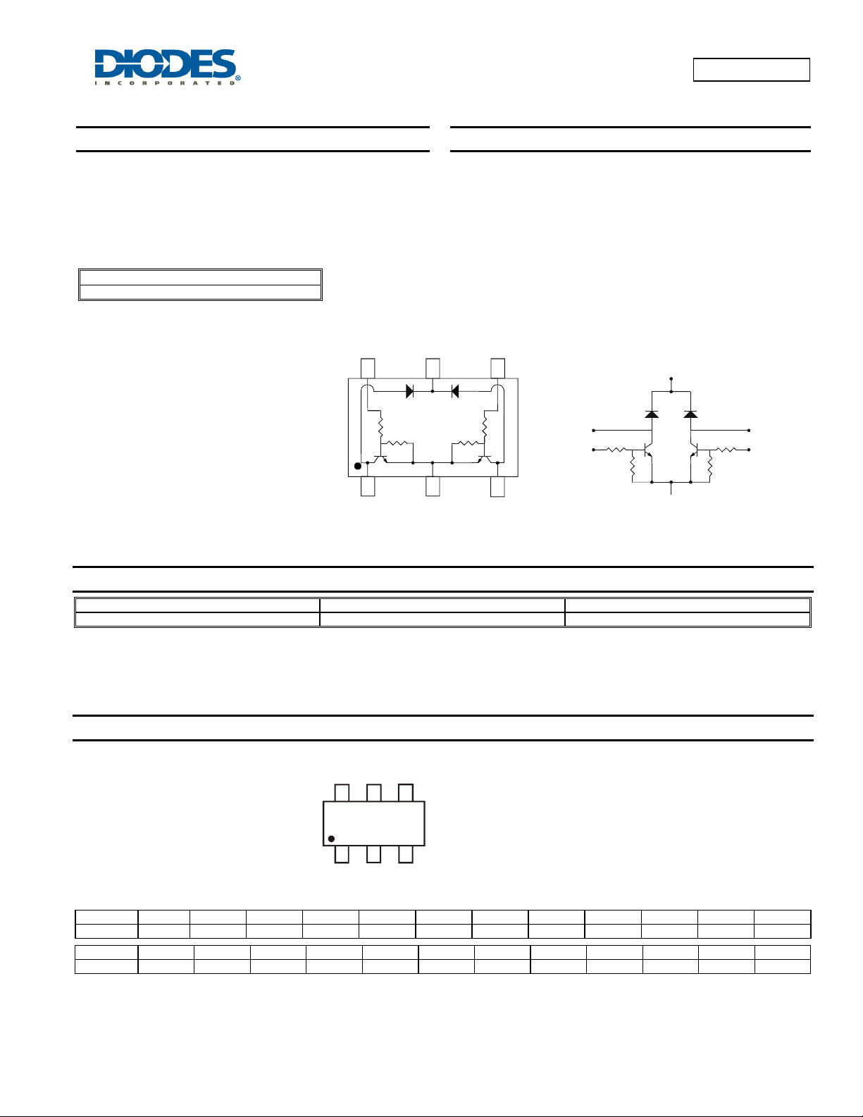
R1 = R3 = 2.2kΩ (nominal)
R2 = R4 = 47kΩ (nominal)
Top View
6
R1
1
R2
Top View
DRDNB21D
COMPLEX ARRAY FOR DUAL RELAY DRIVER
Mechanical Data
• Case: SOT-363
• Case Material: Molded Plastic. "Green" Molding Compound. UL
Flammability Classification Rating 94V-0
• Moisture Sensitivity: Level 1 per J-STD-020
• Terminal Connections: See Diagram
• Terminals: Finish - Matte Tin annealed over Alloy 42 leadframe.
Solderable per MIL-STD-202, Method 208
• Weight: 0.0062 grams (approximate)
R4
R3
4
1
6
R2 R4
3
D1
5
Q1 Q2
2
D2
R3R1
Device Circuit
5
2
3
4
Ordering Information (Note 3)
Device Packaging Shipping
DRDNB21D-7 SOT-363 3000/Tape & Reel
Notes: 1. No purposefully added lead.
2. Diodes Inc.`s “Green” Policy can be found on our website at http://www.diodes.com
3. For packaging details, visit our website at http://www.diodes.com.
Marking Information
RD08
RD08 = Product Type Marking Code
YM = Date Code Marking
Y = Year (e.g. T = 2006)
YM
M = Month (e.g. 1 = January)
Date Code Key
Year 2005 2006 2007 2008 2009 2010 2011 2012 2013 2014 2015 2016
Code S T U V W X Y Z A B C D
Month Jan Feb Mar Apr May Jun Jul Aug Sep Oct Nov Dec
Code 1 2 3 4 5 6 7 8 9 O N D
DRDNB21D
Document number: DS30756 Rev. 6 - 2
1 of 7
www.diodes.com
February 2011
© Diodes Incorporated
Page 2
θ
)
)
)
)
)
Δ
Δ
Maximum Ratings, Total Device @T
= 25°C unless otherwise specified
A
Characteristic Symbol Value Unit
Power Dissipation (Note 4)
Thermal Resistance, Junction to Ambient Air (Note 4)
Operating and Storage Junction Temperature Range
T
J
Maximum Ratings, Pre-Biased NPN Transistor @T
Characteristic Symbol Value Unit
Collector-Emitter Voltage
Base-Emitter Voltage
Output Current
Peak Collector Current
Maximum Ratings, Switching Diode @T
Characteristic Symbol Value Unit
Non-Repetitive Peak Reverse Voltage
Peak Repetitive Reverse Voltage
Working Peak Reverse Voltage
DC Blocking Voltage
RMS Reverse Voltage
Forward Continuous Current (Note 4)
Average Rectified Output Current (Note 4)
Non-Repetitive Peak Forward Surge Current @ t = 1.0μs
@ t = 1.0s
= 25°C unless otherwise specified
A
V
V
V
P
D
R
JA
, T
STG
= 25°C unless otherwise specified
A
V
CC
V
in
I
O
I
CM
V
RM
RRM
RWM
V
R
R(RMS
I
FM
I
O
I
FSM
200 mW
625
-55 to +150
50 V
-5 to +12 V
100 mA
100 mA
100 V
75 V
53 V
500 mA
250 mA
4.0
1.0
DRDNB21D
°C/W
°C
A
Electrical Characteristics, Pre-Biased NPN Transistor @T
= 25°C unless otherwise specified
A
Characteristic Symbol Min Typ Max Unit Test Condition
V
Input Voltage
Output Voltage
Input Current
Output Current
DC Current Gain
Input Resistor Tolerance
Resistance Ratio Tolerance
Gain-Bandwidth Product*
* Transistor - For Reference Only
l(off
V
l(on
V
O(on
I
l
I
O(off
G
l
R1
R2/R1
f
⎯
T
Electrical Characteristics, Switching Diode @T
0.5
⎯ ⎯
⎯ ⎯
⎯ ⎯
⎯ ⎯
80
-30
-20
= 25°C unless otherwise specified
A
⎯ ⎯
1.1 V
0.3 V
3.6 mA
0.5 uA
⎯ ⎯ ⎯
+30 % -
⎯
+20 % -
⎯
250
⎯
V
VCC = 5V, IO = 100μA
VO = 0.3V, IO = 5mA
IO/Il = 50mA/0.25mA
VI = 5V
VCC = 50V, VI = 0V
VO = 5V, IO = 10mA
MHz
VCE = 10V, IE = 5mA, f = 100MHz
Characteristic Symbol Min Max Unit Test Condition
Reverse Breakdown Voltage (Note 5)
Forward Voltage
Reverse Current (Note 5)
Total Capacitance
Reverse Recovery Time
Notes: 4. Device mounted on FR-4 PCB, 1 inch x 0.85 inch x 0.062 inch; pad layout as shown on Diodes Inc. suggested pad layout document AP02001, which
can be found on our website at http://www.diodes.com
5. Short duration pulse test used to minimize self-heating effect.
DRDNB21D
Document number: DS30756 Rev. 6 - 2
V
(BR)R
VF
IR
CT ⎯
trr
www.diodes.com
75
0.62
⎯
⎯
⎯
⎯
⎯
2 of 7
⎯
0.72
0.855
1.0
1.25
2.5
50
30
25
4.0 pF
4.0 ns
V
IR = 10μA
IF = 5.0mA
IF = 10mA
V
IF = 100mA
IF = 150mA
VR = 75V
μA
VR = 75V, TJ = 150°C
μA
μA
VR = 25V, TJ = 150°C
nA
VR = 20V
VR = 0, f = 1.0MHz
IF = IR = 10mA, I
= 0.1 x IR, RL = 100Ω
rr
February 2011
© Diodes Incorporated
Page 3
P, P
OWER
P
T
O
C
O
CTO
R
T
TER
C
C
U
R
R
T G
Device Characteristics
250
200
N (mW)
I
150
A
DISSI
100
D
50
0
0
T , AMBIENT TEMPERATURE (°C)
A
Fig. 1 Power Derating Curve (Total Device)
120
Note 4
1608040
DRDNB21D
200
Pre-Biased NPN Transistor Elements
1
I/I = 10
CB
-EMI
0.1
T = 25C
°
A
T = 75C
°
A
T = -25C
°
A
LLE
0.01
SATURATION VOLT AGE (V)
CE(SAT)
V,
0.001
0
10
I , COLLECTOR CURRENT (mA)
C
20
Fig. 2 Typical V vs. I
30
CE(SAT) C
40
50
DRDNB21D
Document number: DS30756 Rev. 6 - 2
3 of 7
www.diodes.com
1,000
AIN
EN
100
FE
h, D
10
110100
I , COLLECTOR CURRENT (mA)
C
Fig. 3 Typical DC Current Gain
February 2011
© Diodes Incorporated
Page 4

C
O
CTO
R
CUR
REN
T
C, CAPACITANC
F
Pre-Biased NPN Transistor Elements - continued
100
10
(mA)
1
0.1
LLE
0.01
C
I,
0.001
1
0
4
234
V , INPUT VOLTAGE (V)
Fig. 4 Typical Collector Current vs. Input Voltage
in
5
67
89
I = 0mA
E
f = 1MHz
10
DRDNB21D
10
1
in
V , INPUT VOLTAGE (V)
0.1
01020304050
I , COLLECTOR CURRENT (mA)
C
Fig. 5 Typical Input Voltage vs. Collector Curre nt
)
3
E (p
2
OB
1
0
0
10
5
V , REVERSE BIAS VOLTAGE (V)
R
Fig. 6 Typical Output Capacitance
15
20
25
30
DRDNB21D
Document number: DS30756 Rev. 6 - 2
4 of 7
www.diodes.com
February 2011
© Diodes Incorporated
Page 5

NSTAN
TANEO
US FORWAR
CUR
REN
T
TANT
O
US R
R
C
URRENT
C, TOT
CAPACITANC
F
Switching Diode Elements
1,000
(mA)
100
D
10
1
F
I, I
0.1
0
V , I NSTANTANEOUS FORWARD VOLTAGE ( V)
0.4 0.8
F
Fig. 7 Typical Forward C haracteristics
3.0
2.5
)
1.2
f = 1MHz
1.6
10,000
(nA )
1,000
SE
EVE
ANE
R
I, INS
100
10
0.1
DRDNB21D
1
0
20 40
V , REVERSE VOLTAGE (V)
R
Fig. 8 Typical Reverse Characteristics
60 80 100
E (p
2.0
1.5
AL
1.0
T
0.5
0
01020 40
V , REVERSE VOLTAGE (V)
R
30
Fig. 9 Typical Capacitance vs. Reverse Voltage
Typical Application Circuit
Relay1
Typical Application Circuit DRDNB21D with two independent relays.
DRDNB21D
Document number: DS30756 Rev. 6 - 2
RL1
L1
D1
5 of 7
www.diodes.com
February 2011
© Diodes Incorporated
Page 6

Package Outline Dimensions
K
J
A
B C
H
D
F
Suggested Pad Layout
G
Z
Y
C2
X
DRDNB21D
SOT-363
Dim Min Max
A 0.10 0.30
B 1.15 1.35
C 2.00 2.20
D 0.65 Typ
F 0.40 0.45
H 1.80 2.20
M
L
C2
Dimensions Value (in mm)
C1
J 0 0.10
K 0.90 1.00
L 0.25 0.40
M 0.10 0.22
α
All Dimensions in mm
Z 2.5
G 1.3
X 0.42
Y 0.6
C1 1.9
C2 0.65
0° 8°
DRDNB21D
Document number: DS30756 Rev. 6 - 2
6 of 7
www.diodes.com
February 2011
© Diodes Incorporated
Page 7

IMPORTANT NOTICE
DIODES INCORPORATED MAKES NO WARRANTY OF ANY KIND, EXPRESS OR IMPLIED, WITH REGARDS TO THIS DOCUMENT,
INCLUDING, BUT NOT LIMITED TO, THE IMPLIED WARRANTIES OF MERCHANTABILITY AND FITNESS FOR A PARTICULAR PURPOSE
(AND THEIR EQUIVALENTS UNDER THE LAWS OF ANY JURISDICTION).
Diodes Incorporated and its subsidiaries reserve the right to make modifications, enhancements, improvements, corrections or other changes
without further notice to this document and any product described herein. Diodes Incorporated does not assume any liability arising out of the
application or use of this document or any product described herein; neither does Diodes Incorporated convey any license under its patent or
trademark rights, nor the rights of others. Any Customer or user of this document or products described herein in such applications shall assume
all risks of such use and will agree to hold Diodes Incorporated and all the companies whose products are represented on Diodes Incorporated
website, harmless against all damages.
Diodes Incorporated does not warrant or accept any liability whatsoever in respect of any products purchased through unauthorized sales channel.
Should Customers purchase or use Diodes Incorporated products for any unintended or unauthorize d application, Customers shall indemnify and
hold Diodes Incorporated and its representatives harmless against all claims, damages, expenses, and attorney fees arising out of, directly or
indirectly, any claim of personal injury or death associated with such unintended or unauthorized application.
Products described herein may be covered by one or more United States, international or foreign patents pending. Product names and markings
noted herein may also be covered by one or more United States, international or foreign trademarks.
LIFE SUPPORT
Diodes Incorporated products are specifically not authorized for use as critical components in life support devices or systems without the express
written approval of the Chief Executive Officer of Diodes Incorporated. As used herein:
A. Life support devices or systems are devices or systems which:
1. are intended to implant into the body, or
2. support or sustain life and whose failure to perform when properly used in accordance with instructions for use provided in the
labeling can be reasonably expected to result in significant injury to the user.
B. A critical component is any component in a life support device or system whose failure to perform can be reasonably expected to cause the
failure of the life support device or to affect its safety or effectiveness.
Customers represent that they have all necessary expertise in the safety and regulatory ramifications of their life support devices or systems, and
acknowledge and agree that they are solely responsible for all legal, regulatory and safety-related requirements concerning their products and any
use of Diodes Incorporated products in such safety-critical, life support devices or systems, notwithstanding any devices- or systems-related
information or support that may be provided by Diodes Incorporated. Further, Customers must fully indemnify Diodes Incorporated and its
representatives against any damages arising out of the use of Diodes Incorporated products in such safety-critical, life support devices or systems.
Copyright © 2011, Diodes Incorporated
www.diodes.com
DRDNB21D
DRDNB21D
Document number: DS30756 Rev. 6 - 2
7 of 7
www.diodes.com
February 2011
© Diodes Incorporated
 Loading...