Diodes DPLS350Y User Manual

Features
BV
I
I
2W Power Dissipation
Low Saturation Voltage V
R
Totally Lead-Free & Fully RoHS compliant (Notes 1 & 2)
Halogen and Antimony Free. “Green” Device (Note 3)
Qualified to AEC-Q101 Standards for High Reliability
> -50V
CEO
= -3A High Continuous Collector Current
C
up to -5A Peak Pulse Current
CM
< -180mV @ 1A
= 67m @ 2A for a Low Equivalent On-Resistance
CE(sat)
CE(sat)
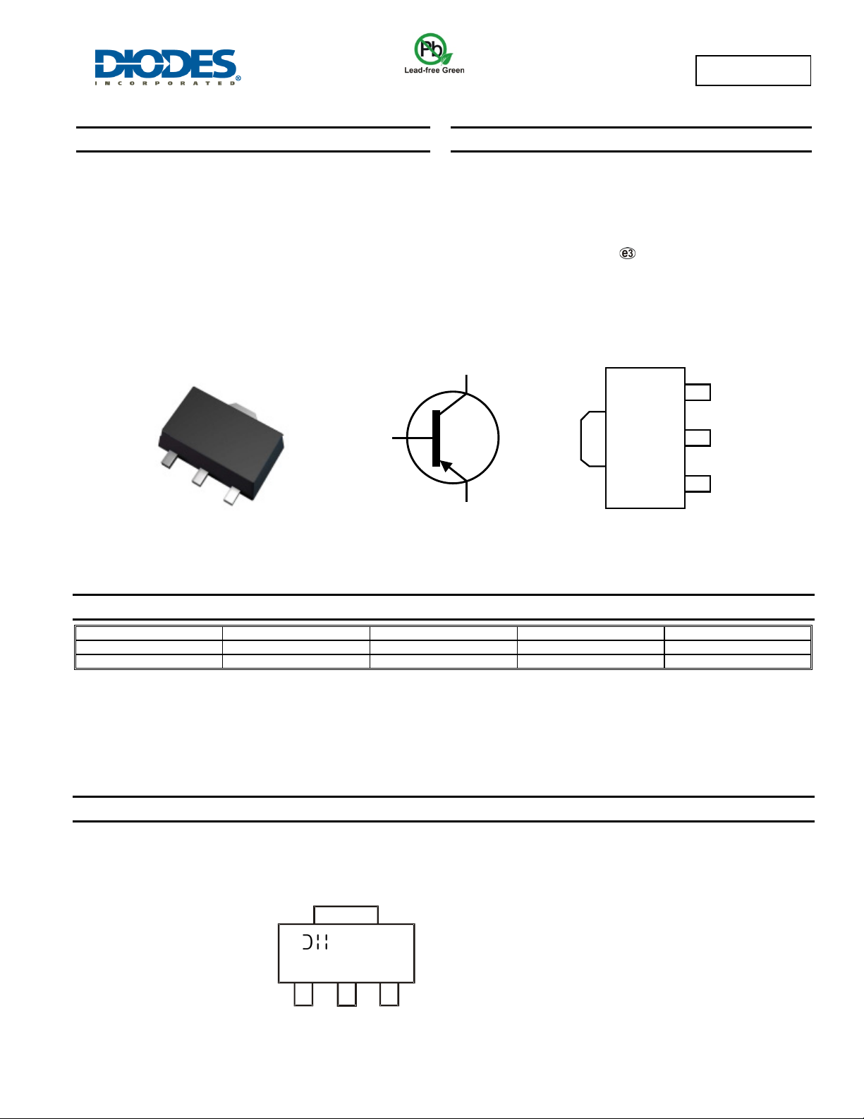
SOT89
B
DPLS350Y
50V PNP LOW SATURATION POWER TRANSISTOR IN SOT89
Mechanical Data
Case: SOT89
Case Material: Molded Plastic, “Green” Molding Compound
UL Flammability Rating 94V-0
Moisture Sensitivity: Level 1 per J-STD-020
Terminals: Finish - Matte Tin Plated Leads, Solderable per
MIL-STD-202, Method 208
Weight: 0.052 grams (Approximate)
C
E
C
C
B
Top View
Device Symbol
E
Top View
Pin-Out
Ordering Information (Note 4)
Part Number Marking Reel size (inches) Tape width (mm) Quantity per reel
DPLS350Y-13 P35 13 12 2,500
DPLS350Y-13R P35 13 12 4,000
Notes: 1. No purposely added lead. Fully EU Directive 2002/95/EC (RoHS) & 2011/65/EU (RoHS 2) compliant.
3. Halogen and Antimony free "Green” products are defined as those which contain <900ppm bromine, <900ppm chlorine (<1500ppm total Br + Cl) and
4. For packaging details, go to our website at http://www.diodes.com/products/packages.html
2. See http://www.diodes.com/quality/lead_free.html for more information about Diodes Incorporated’s definitions of Halogen and Antimony free,"Green"
and Lead-Free.
<1000ppm antimony compounds.
Marking Information
(Top View)
YWW
P35
P35 = Product Type Marking Code:
YWW = Date Code Marking
Y = Last digit of year ex: 1 = 2011
WW = Week code 01 - 52
DPLS350Y
Document number: DS31149 Rev. 6 - 2
1 of 6
www.diodes.com
February 2013
© Diodes Incorporated

Maximum Ratings (@T
Collector-Base Voltage
Collector-Emitter Voltage
Emitter-Base Voltage
Continuous Collector Current
Peak Pulse Current
Base Current
Thermal Characteristics (@T
Power Dissipation
Thermal Resistance, Junction to Ambient Air
Thermal Resistance, Junction to Leads (Note 7)
Operating and Storage Temperature Range
Notes: 5. For a device surface mounted on 15mm x 15mm x 0.6mm FR4 PCB with high coverage of single sided 1 oz copper, in still air conditions; the device is
measured when operating in steady state condition.
6. Same as note (5), except the device is mounted on 40mm x 40mm x 1.6mm FR4 PCB.
7. Thermal resistance from junction to solder-point (on the exposed collector pad).
= +25°C, unless otherwise specified.)
A
Characteristic Symbol Value Unit
V
CBO
V
CEO
V
EBO
I
C
I
CM
I
B
= +25°C, unless otherwise specified.)
A
Characteristic Symbol Value Unit
(Note 5)
(Note 6) 2
(Note 5)
(Note 6) 62.5
P
R
JA
R
T
J,TSTG
JL
D
-50 V
-50 V
-6 V
-3 A
-5 A
-500 mA
1
125
5.73 °C/W
-55 to +150 °C
DPLS350Y
W
°C/W
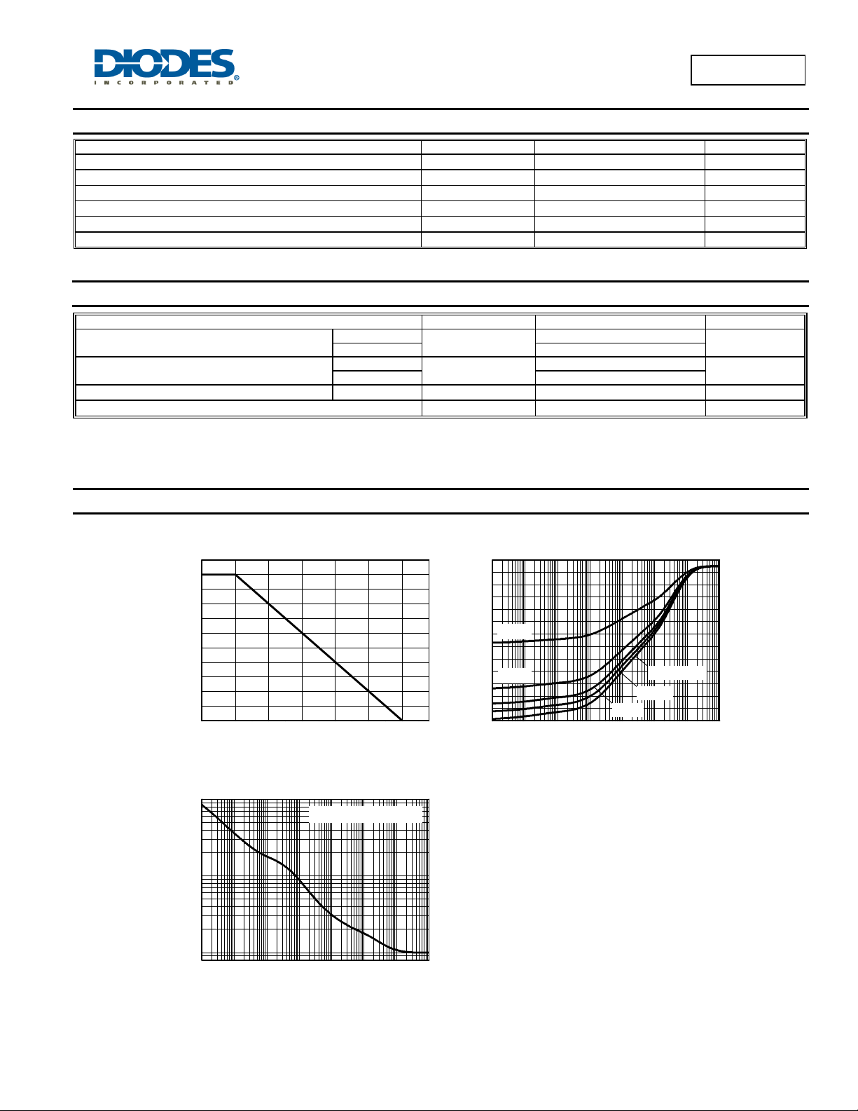
Thermal Characteristics and Derating Information
1.0
0.8
0.6
0.4
0.2
0.0
0 25 50 75 100 125 150
Max Power Dissipation (W)
Temperature (°C)
Derating Curve
100
Single Pulse. T
10
amb
=25°C
Thermal Resistance (°C/W)
120
100
80
D=0.5
60
40
D=0.2
20
0
100µ 1m 10m 100m 1 10 100 1k
Single Pulse
D=0.05
D=0.1
Pulse Width (s)
Transient Thermal Impedance
1
100µ 1m 10m 100m 1 10 100 1k
Max Power Dissipation (W)
Pulse Width (s)
Pulse Power Dissipation
DPLS350Y
Document number: DS31149 Rev. 6 - 2
2 of 6
www.diodes.com
February 2013
© Diodes Incorporated
 Loading...