

Page 1
Features
• P-Channel MOSFET
• Very Low On-Resistance
• Very Low Gate Threshold Voltage
• Low Input Capacitance
• Fast Switching Speed
• Low Input/Output Leakage
• Ultra-Small Surface Mount Package
• Lead Free By Design/RoHS Compliant (Note 2)
• "Green" Device (Note 3)
• Qualified to AEC-Q101 Standards for High Reliability
NEW PRODUCT
Maximum Ratings @T
Drain-Source Voltage
Gate-Source Voltage
Continuous Drain Current (Note 1)
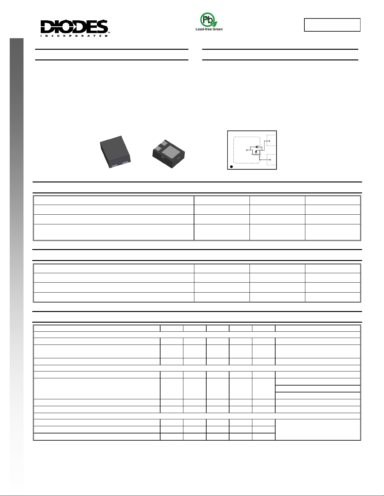
TOP VIEW
= 25°C unless otherwise specified
A
Characteristic Symbol Value Units
DMP2104LP
P-CHANNEL ENHANCEMENT MODE FIELD EFFECT TRANSISTOR
Mechanical Data
• Case: DFN1411-3
• Case Material: Molded Plastic, “Green” Molding
Compound. UL Flammability Classification Rating 94V-0
• Moisture Sensitivity: Level 1 per J-STD-020C
• Terminal Connections: See Diagram
• Terminals: Finish - NiPdAu over Copper lead frame.
Solderable per MIL-STD-202, Method 208
• Marking Information: See Page 3
• Ordering Information: See Page 3
• Weight: 0.003 grams (approximate)
DFN1411-3
S
D
G
BOTTOM VIEW
TA = 25°C
T
= 70°C
A
V
DSS
V
GSS
I
D
TOP VIEW
Internal Schematic
-20 V
±12 V
-1.5
-1.2
A
Thermal Characteristics @T
= 25°C unless otherwise specified
A
Characteristic Symbol Value Units
Power Dissipation (Note 1)
Thermal Resistance, Junction to Ambient (Note 1)
Operating and Storage Temperature Range
Electrical Characteristics @T
= 25°C unless otherwise specified
A
Characteristic Symbol Min Typ Max Unit Test Condition
OFF CHARACTERISTICS (Note 4)
Drain-Source Breakdown Voltage
Zero Gate Voltage Drain Current TJ = 25°C
T
= 125°C
J
Gate-Source Leakage
ON CHARACTERISTICS (Note 4)
Gate Threshold Voltage
Static Drain-Source On-Resistance
R
Forward Transconductance
Diode Forward Voltage (Note 4)
DYNAMIC CHARACTERISTICS
Input Capacitance
Output Capacitance
Reverse Transfer Capacitance
Notes: 1. Device mounted on FR-4 PCB with 1 inch square pads.
2. No purposefully added lead.
3. Diodes Inc.’s “Green” policy can be found on our website at http://www.diodes.com/products/lead_free/index.php.
4. Short duration pulse test used to minimize self-heating effect.
DMP2104LP
Document number: DS31091 Rev. 6 - 2
BV
DSS
I
DSS
I
GSS
V
GS(th)
DS (ON)
g
V
C
C
C
-0.45
FS
SD
iss
oss
rss
www.diodes.com
T
-20
⎯ ⎯
⎯ ⎯
⎯
134
180
⎯
⎯ ⎯
⎯
320
⎯
⎯
1 of 4
P
D
R
JA
θ
j, TSTG
⎯ ⎯
-1.0
-5.0
±100
⎯
92
-1.0 V
150
200
240
3.1
-0.9 V
80
60
⎯
⎯
⎯
⎯
500 mW
250 °C/W
-55 to +150 °C
V
V
= 0V, ID = -250μA
GS
μA
V
= -20V, VGS = 0V
DS
nA
V
= ±12V, VDS = 0V
GS
V
= VGS, ID = -250μA
DS
VGS = -4.5V, ID = -950mA
mΩ
VGS = -2.5V, ID = -670mA
V
= -1.8V, ID = -200mA
GS
S
V
= -10V, ID = -810mA
DS
V
= 0V, IS = -360mA
GS
pF
pF
pF
= -16V, VGS = 0V
V
DS
f = 1.0MHz
November 2007
© Diodes Incorporated
Page 2
NEW PRODUCT
DMP2104LP
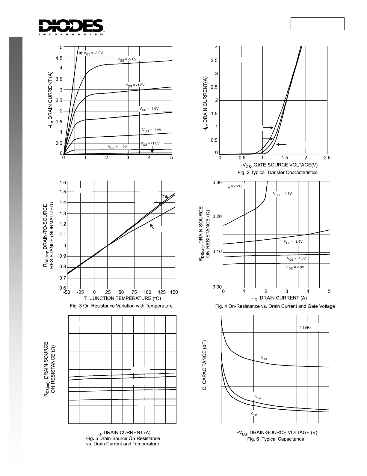
V = -10V
DS
T = 125°C
A
T = 25°C
-V , DRAIN-SOURCE VOLTAGE(V)
DS
Fig.1 Typical Out put Characteristics
I = 1.0A
D
V = -2.5V
GS
V = -4.5V
GS
A
T = -55°C
A
0.30
0.20
0.10
V = -4.5V
GS
T = 150°C
A
T = 125°C
A
T = 25°C
A
T = -55°C
A
V = -1.8V
GS
600
500
400
300
200
100
0.00
012 34
DMP2104LP
Document number: DS31091 Rev. 6 - 2
5
2 of 4
www.diodes.com
0
024 6810121416182
November 2007
© Diodes Incorporated
0
Page 3

NEW PRODUCT
0.3
0.27
0.24
0.21
0.18
0.15
0.12
0.09
0.06
0.03
0
-50 -25 0 25 50 75 100 125 150
1
10,000
1,000
100
2 4 6 8 10 12 14 16 18 20
DMP2104LP
V = 0V
0.8
0.6
0.4
0.2
0
GS
T = 25°C
j
0 0.2 0.4 0.6 0.8 1
Ordering Information (Note 5)
Part Number Case Packaging
DMP2104LP-7 DFN1411-3 3000/Tape & Reel
Notes: 5. For packaging details, go to our website at http://www.diodes.com/datasheets/ap02007.pdf.
Marking Information
Date Code Key
Year 2007 2008 2009 2010 2011 2012
Code U V W X Y Z
Month Jan Feb Mar Apr May Jun Jul Aug Sep Oct Nov Dec
Code 1 2 3 4 5 6 7 8 9 O N D
PA
DMP2104LP
Document number: DS31091 Rev. 6 - 2
PA = Marking Code
YM = Date Code Marking
Y = Year ex: U = 2007
YM
M = Month ex: 9 = September
3 of 4
www.diodes.com
November 2007
© Diodes Incorporated
Page 4

DMP2104LP
Package Outline Dimensions
NEW PRODUCT
G
H
DFN1411-3
Dim Min Max Typ
A 1.35 1.48 1.40
B 1.05 1.18 1.10
C 0.65 0.85 0.75
D
⎯ ⎯
E
⎯ ⎯
F
⎯ ⎯
G 0.47 0.53 0.50
H 0 0.05 0.02
K 0.25 0.35 0.30
L 0.22 0.33 0.275
M
⎯ ⎯
N
⎯ ⎯
All Dimensions in mm
0.125
0.25
0.175
0.55
0.20
Suggested Pad Layout
Diodes Incorporated and its subsidiaries reserve the right to make modifications, enhancements, improvements, corrections or other changes
without further notice to any product herein. Diodes Incorporated does not assume any liability arising out of the application or use of any product
described herein; neither does it convey any license under its patent rights, nor the rights of others. The user of products in such applications shall
assume all risks of such use and will agree to hold Diodes Incorporated and all the companies whose products are represented on our website,
harmless against all damages.
Diodes Incorporated products are not authorized for use as critical components in life support devices or systems without the expressed written
approval of the President of Diodes Incorporated.
X1
C
X2
X
G2
Y
G1
Z
Dimensions Value (in mm)
Z 1.38
G1 0.15
G2 0.15
X 0.95
X1 0.75
X2 0.40
Y 0.75
C 0.76
IMPORTANT NOTICE
LIFE SUPPORT
DMP2104LP
Document number: DS31091 Rev. 6 - 2
4 of 4
www.diodes.com
November 2007
© Diodes Incorporated
 Loading...