Diodes DMP2070UCB6 User Manual

NEW PRODUCT
Product Summary
I
V
R
(BR)DSS
-20V
70m @ V
90m @ VGS = -2.5V
DS(ON)
GS
= -4.5V
D
TA = 25°C
3.5 A
3.0 A
Description and Applications
This new generation MOSFET has been designed to minimize the onstate resistance (R
performance, making it ideal for high efficiency power management
applications.
• Battery Management
• Load Switch
• Battery Protection
) and yet maintain superior switching
DS(on)
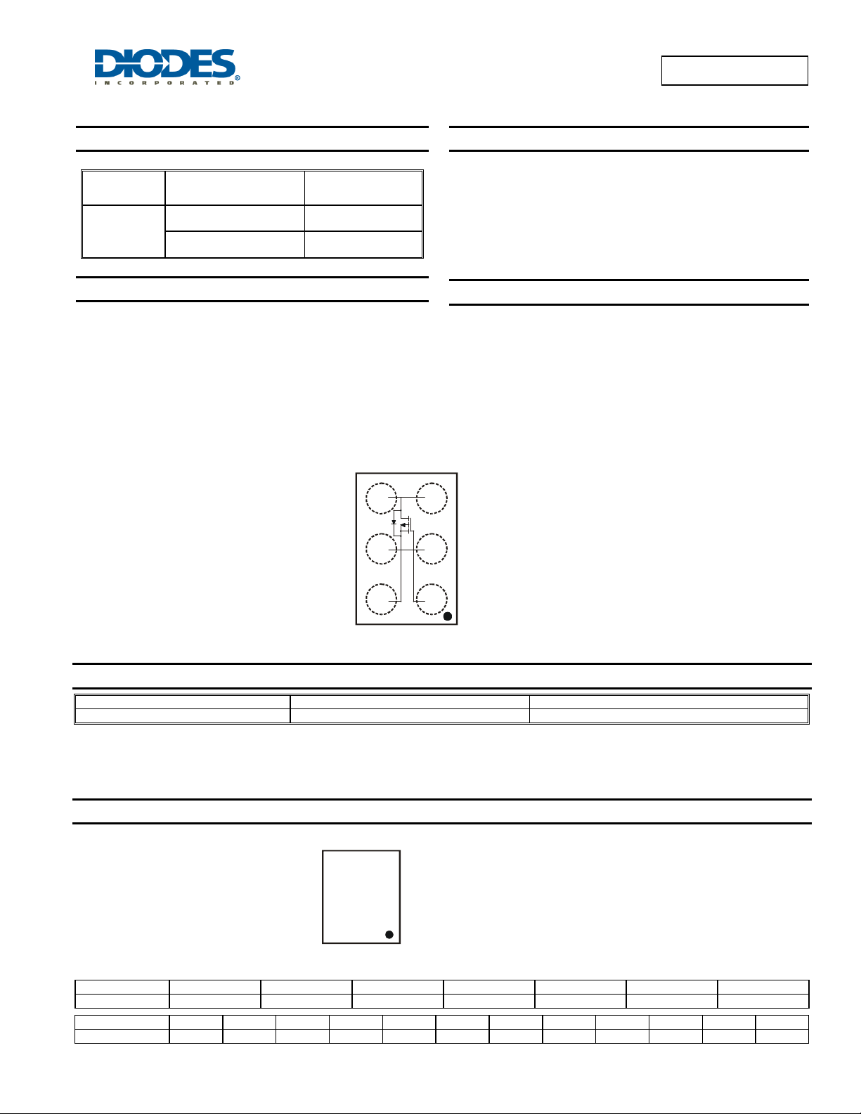
U-WLB1510-6
DD
SS
SG
Top View
DMP2070UCB6
P-CHANNEL ENHANCEMENT MODE MOSFET
Features and Benefits
• Low Qg & Qgd
• Small Footprint
• Low Profile 0.62mm height
• Lead Free By Design/RoHS Compliant (Note 1)
• "Green" Device Halogen and Antimony Free (Note 2)
• Qualified to AEC-Q101 Standards for High Reliability
Mechanical Data
• Case: U-WLB1510-6
• Terminal Connections: See Diagram Below
• Weight: 0.0018 grams (approximate)
Ordering Information (Note 3)
Part Number Case Packaging
DMP2070UCB6-7 U-WLB1510-6 3000/Tape & Reel
Notes: 1. No purposefully added lead.
2. Diodes Inc.’s “Green” policy can be found on our website at http://www.diodes.com.
3. For packaging details, go to our website at http://www.diodes.com
Marking Information
Date Code Key
Year 2011 2012 2013 2014 2015 2016 2017
Code Y Z A B C D E
Month Jan Feb Mar Apr May Jun Jul Aug Sep Oct Nov Dec
Code 1 2 3 4 5 6 7 8 9 O N D
2W
2W = Product Type Marking Code
YM = Date Code Marking
Y = Year (ex: Y = 2011)
YM
M = Month (ex: 9 = September)
DMP2070UCB6
Document number: DS35553 Rev. 2 - 2
1 of 6
www.diodes.com
October 2011
© Diodes Incorporated

θ
θ
)
g
g
g
)
r
)
NEW PRODUCT
Maximum Ratings @T
Drain-Source Voltage
Gate-Source Voltage
Continuous Drain Current (Note 4) VGS = -4.5V
Continuous Drain Current (Note 5) VGS = -4.5V
Pulsed Drain Current (Note 6)
Maximum Continuous Body Diode Forward Current (Note 5)
Thermal Characteristics @T
Total Power Dissipation (Note 4)
Total Power Dissipation (Note 5)
Thermal Resistance, Junction to Ambient (Note 4)
Thermal Resistance, Junction to Ambient (Note 5)
Operating and Storage Temperature Range
= 25°C unless otherwise specified
A
Characteristic Symbol Value Units
Steady
State
Steady
State
= 25°C unless otherwise specified
A
Characteristic Symbol Value Units
T
= 25°C
A
T
= 70°C
A
T
= 25°C
A
= 70°C
T
A
P
P
R
R
T
J, TSTG
DMP2070UCB6
V
DSS
V
GSS
I
D
I
D
I
DM
I
S
D
D
JA
JA
-55 to +150 °C
-20 V
±8 V
-2.5
-2.0
-3.5
-2.8
A
A
-12 A
-1.8 A
0.92 W
1.47 W
136 °C/W
84 °C/W
Electrical Characteristics @T
= 25°C unless otherwise specified
A
Characteristic Symbol Min Typ Max Unit Test Condition
OFF CHARACTERISTICS (Note 7)
Drain-Source Breakdown Voltage
Zero Gate Voltage Drain Current @TC = 25°C I
Gate-Source Leakage
BV
DSS
I
GSS
DSS
-20 - - V
- - -1 A
- - ±100 nA
VGS = 0V, ID = -250A
VDS = -16V, VGS = 0V
VGS = ±8V, VDS = 0V
ON CHARACTERISTICS (Note 7)
Gate Threshold Voltage
Static Drain-Source On-Resistance
Forward Transfer Admittance
Diode Forward Voltage (Note 5)
V
GS(th
R
DS (ON)
|Y
V
SD
-0.4 -0.6 -1.0 V
55 70
90 110
70 90
110 150
|
fs
- 12 - S
- -0.7 -1 V
VDS = VGS, ID = -250A
= -4.5V, ID = - 1A
V
GS
V
= -2.5V, ID = -1A
mΩ
GS
V
= -1.8V, ID = -1A
GS
V
= -1.5V, ID = -1A
GS
VDS = -10V, ID = -1A
VGS = 0V, IS = -1A
DYNAMIC CHARACTERISTICS (Note 8)
Input Capacitance
Output Capacitance
Reverse Transfer Capacitance
Series Gate Resistance
Total Gate Charge (4.5V)
Gate-Source Charge
Gate-Drain Charge
Turn-On Delay Time
Turn-On Rise Time
Turn-Off Delay Time
Turn-Off Fall Time
Notes: 4. Device mounted on FR-4 PCB with minimum recommended pad layout.
5. Device mounted on FR4 material with 1-inch
6 300ms pulse, pulse duty cycle 2%
7. Short duration pulse test used to minimize self-heating effect.
8. Guaranteed by design. Not subject to production testing.
2
(6.45-cm2), 2-oz. (0.071-mm thick) Cu
C
C
C
Q
Q
t
D(on
t
D(off
iss
oss
rss
R
G
Q
t
t
f
s
d
- 210 - pF
- 92 - pF
- 38 - pF
5.3 -
- 2.9 - nC
- 0.3 - nC
- 0.5 - nC
- 7.3 - ns
- 14.0 - ns
- 42.6 - ns
- 32 - ns
= -10V, VGS = 0V,
V
DS
f = 1.0MHz
Ω
VDS = 0V, VGS = 0V, f = 1MHz
V
= -4.5V, VDS = -10V,
GS
I
= -1A ,
D
V
= -10V, VGS = -4.5V,
DD
= -1A, RG = 20,
I
DS
DMP2070UCB6
Document number: DS35553 Rev. 2 - 2
2 of 6
www.diodes.com
October 2011
© Diodes Incorporated
 Loading...