

Page 1
f
n
Summary
V
R
(BR)DSS
29mΩ @V
-12V
45mΩ @V
60mΩ @V
100mΩ @V
max I
DS(on)
= -4.5V
GS
= -2.5V
GS
= -1.8V
GS
= -1.5V
GS
Application
This device provides a high performance, low R
MOSFETs in the thermally and space efficient X1-DFN1616-6
package. The low R
losses are kept making it ideal for use as a:
• Battery disconnect switch
• Load switch for power management functions
ADVANCE INFORMATION
of this MOSFET ensures conduction
DS(ON)
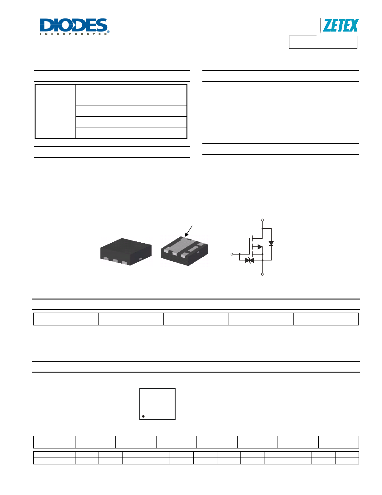
Top View
max
D
-6.6 A
-5.3 A
-4.6 A
-3.5 A
P channel
DS(ON)
X1-DFN1616-6
Type E
A Product Line o
Diodes Incorporated
DMP1245UFCL
12V P-CHANNEL ENHANCEMENT MODE MOSFET
Features and Benefits
• Typical off board profile of 0.5mm - ideally suited for thin
applications
• Low R
• PCB footprint of 2.56mm
• 3kV ESD Protected Gate – protected against human borne
ESD
• “Lead-Free”, RoHS Compliant (Note 1)
• "Green" Device (Note 2)
– minimizes conduction losses
DS(ON)
2
Mechanical Data
• Case: X1-DFN1616-6 Type E
• Case Material: Molded Plastic, “Green” Molding Compound.
UL Flammability Classification Rating 94V-0
• Moisture Sensitivity: Level 1 per J-STD-020
• Lead Free Plating (NiPdAu Finish over Copper leadframe).
• Terminals: Solderable per MIL-STD-202, Method 208
• Weight: 0.04 grams (approximate)
Drai
Pin 1
Gate
Gate
Protection
Diode
Device symbol Bottom View
Source
Top View
Pin-Out
Ordering Information (Note 3)
Product Marking Reel size (inches) Tape width (mm) Quantity per reel
DMP1245UFCL-7 P5 7 8 3,000
Notes: 1. No purposefully added lead.
2. Diodes Inc’s “Green” Policy can be found on our website at http://www.diodes.com
3. For packaging details, go to our website at http://www.diodes.com
Marking Information
Date Code Key
Year 2011 2012 2013 2014 2015 2016 2017
Code Y Z A B C D E
Month Jan Feb Mar Apr May Jun Jul Aug Sep Oct Nov Dec
Code 1 2 3 4 5 6 7 8 9 O N D
P5
YM
DMP1245UFCL
Document number: DS35505 Rev. 1 - 2
P5 = Product Type Marking Code
YM = Date Code Marking
Y = Year (ex: X = 2010)
M = Month (ex: 9 = September)
1 of 7
www.diodes.com
November 2011
© Diodes Incorporated
Page 2
f
Diodes Incorporated
DMP1245UFCL
A Product Line o
Maximum Ratings @T
= 25°C unless otherwise specified
A
Characteristic Symbol Value Units
Drain-Source Voltage
Gate-Source Voltage
Continuous Drain Current (Note 5) @TA = 25°C
@T
= 70°C
A
V
DSS
V
GSS
I
D
Pulsed Drain Current TP = 10μs IDM
-12 V
±8 V
-6.6
-5.25
A
-16.67 A
Thermal Characteristics @T
= 25°C unless otherwise specified
A
Characteristic Symbol Value Units
Total Power Dissipation
Thermal Resistance, Junction to Ambient
Operating and Storage Temperature Range
Notes: 4. For a device surface mounted on minimum recommended pad layout, in still air conditions; the device is measured when operating in a steady state
ADVANCE INFORMATION
condition.
5. For a device surface mounted on 25mm by 25mm by 1.6mm FR4 PCB with high coverage of single sided 2oz copper, in still air conditions; the device is
measured when operating in a steady state condition.
(Note 4)
(Note 5) 1.7 W
(Note 4)
(Note 5) 74
P
R
T
J, TSTG
D
JA
θ
613 mW
204
°C/W
-55 to +150 °C
Thermal Characteristics
100
90
80
70
60
50
40
30
20
P(pk), PEAK TRANSIENT POWER (W)
10
0
0.0001 0.001 0.01 0.1 1 10 100 1000
t , PULSE DURA TION TIME (sec)
1
Fig. 1 Single Pulse Maximum Power Dissipation
Single Pulse
R =205°C/W
θ
JA
R(t)=R*r(t)
θθ
JA JA
T-T=P*R (t)
θ
JA JA
100
D
I , DRAIN CURRENT (A)
10
0.1
R
DS(ON)
Limited
I
D
(
A
)
@
I (A) @ DC
1
T = 150 C
T= 25C
Single Pulse
0.01
D
I (A) @P =10s
DW
I(A) @P =1s
DW
I (A) @P =100ms
DW
I (A) @P =10ms
J(MAX)
A
°
°
DW
0.1 1 10 100
-V , DRAIN-SOURCE VOLTAGE (V)
DS
Fig. 2 SOA, Safe Operat ion Area
I(A) @
D
P =10µs
W
I
D
(
A
)
@
P
W
=
1
m
P
W
s
=
1
0
0
µ
s
DMP1245UFCL
Document number: DS35505 Rev. 1 - 2
2 of 7
www.diodes.com
November 2011
© Diodes Incorporated
Page 3
f
)
g
g
g
)
r
)
Diodes Incorporated
DMP1245UFCL
1
0.1
0.01
A Product Line o
r(t), TRANSIENT THERMAL RESISTANCE
0.001
0.00001 0.0001 0.001 0.01 0.1 1 10 100 1000
ADVANCE INFORMATION
t1, PULSE DURATION TIMES (sec)
R(t)=r(t) * R
θθ
JA JA
R = 205°C/W
θ
JA
Duty Cycle, D=t1/ t2
Fig. 03 Transient Thermal Resist ance
Electrical Characteristics @T
= 25°C unless otherwise specified
A
Characteristic Symbol Min Typ Max Unit Test Condition
OFF CHARACTERISTICS (Note 6)
Drain-Source Breakdown Voltage
Zero Gate Voltage Drain Current TJ = 25°C I
Gate-Source Leakage
BV
I
DSS
DSS
GSS
-12
⎯ ⎯
⎯ ⎯
⎯ ⎯
V
-1 µA
±10
µA
VGS = 0V, ID = -250µA
VDS = -12.0V, VGS = 0V
V
= ±8.0V, VDS = 0V
GS
ON CHARACTERISTICS (Note 6)
Gate Threshold Voltage
Static Drain-Source On-Resistance
Forward Transfer Admittance
Diode Forward Voltage
V
GS(th
R
DS (ON)
|Y
V
fs
SD
-0.3 -0.6 -0.95 V
⎯
⎯
⎯
⎯
0.4 3 - S
|
- - -1.0 V
25 29
31 45
40 60
60 100
VDS = VGS, ID = -250µA
V
= -4.5V, ID = - 4A
GS
= -2.5V, ID = - 3.5A
V
m
GS
= -1.8V, ID = - 1A
V
GS
= -1.5 V, ID = - 0.5A
V
GS
VDS = -5V, ID = -2A
VGS = 0V, ID = -2A
DYNAMIC CHARACTERISTICS (Note 7)
Input Capacitance
Output Capacitance
Reverse Transfer Capacitance
Gate Resistance
Total Gate Charge
Gate-Source Charge
Gate-Drain Charge
Turn-On Delay Time
Turn-On Rise Time
Turn-Off Delay Time
Turn-Off Fall Time
Notes: 6. Short duration pulse test used to minimize self-heating effect.
7. Guaranteed by design. Not subject to production testing.
C
C
t
t
C
oss
rss
R
Q
Q
Q
D(on
t
D(off
t
iss
g
s
d
f
- 1357.4 -
- 499 -
- 273.6 -
- 14.26 -
- 16.1 -
- 26.1 - nC
- 1.71 -
- 20.48 -
- 15.2 -
- 33.11 -
- 219.4 -
- 217.64 -
pF
pF
pF
nC
nC
= -10V, VGS = 0V
V
DS
f = 1.0MHz
VDS = 0V, VGS = 0V, f = 1MHz
= -4.5V
V
GS
= -8V
V
GS
nC
ns
ns
V
= -2.5V, VDS = -10V
GS
ns
= -180mA, RG = 2.0,
I
D
ns
I
= -1A,
D
V
DS
= -10V
DMP1245UFCL
Document number: DS35505 Rev. 1 - 2
3 of 7
www.diodes.com
November 2011
© Diodes Incorporated
Page 4

f
RAIN CUR
R
N
T
R
CUR
RENT
R
RAIN-SOUR
CE O
N-R
TAN
C
R
R
OUR
C
ON-R
TANC
Diodes Incorporated
DMP1245UFCL
A Product Line o
20
V = 1.8V
V = 2.0V
GS
GS
16
(A)
E
12
V = 2.5V
GS
V = 4.5V
GS
V = 1.5V
GS
8
V = 1.2V
GS
-I , D
D
V = 8.0V
4
0
0 0.5 1 1.5 2 2.5 3 3.5 4 4.5 5
GS
-V , DRAIN-SOURCE VOLTAGE (V)
DS
Fig. 4 Typical Output Ch aracteristics
0.06
Ω
ADVANCE INFORMATION
0.05
V = -1.5V
GS
20
16
(A)
12
8
AIN
D
-I , D
4
0
0 0.5 1.0 1.5 2.0 2.5 3.0
-V , GATE-SOURCE VOLT AGE (V)
GS
Fig. 5 Typical Transfer Characteristic
0.06
Ω
V = 4.5V
E ( )
GS
V = -1.8V
0.04
0.03
V = -4.5V
GS
V = -2.5V
GS
GS
V = -3.5V
GS
0.02
0.01
DS(ON)
R , DRAIN-SOURCE ON-RESISTANCE ( )
0
048121620
I , DRAIN-SOURCE CURRENT (A)
D
Fig. 6 Typical On-Resistance
vs. Drain C urrent and G ate V ol tage
1.7
E
1.5
ESIS
V = -2.5V
GS
I = -5A
D
1.3
E
1.1
(NORMALIZED)
0.9
AIN-S
V = -4.5V
GS
I = -10A
D
, D
0.7
DSON
0.5
-50 -25 0 25 50 75 100 125 150
T , AMBIENT TEMPERATURE (°C)
A
Fig. 8 On-Resistance Variation with Temperature
T = 150°C
ESIS
0.04
0.02
T = 85°C
A
T = 125°C
A
T = 25°C
A
A
T = -55°C
A
, D
DS(ON)
0
048121620
I , DRAIN CURRENT (A)
D
Fig. 7 Typical On-Resistance
vs. Drain C urrent and Temperature
0.06
Ω
0.05
V = -2.5V
GS
I = -5A
D
0.04
0.03
V = -4.5V
GS
I = -10A
D
0.02
0.01
DSON
R , DRAIN-SOURCE ON-RESISTANCE ( )
0
-50-250255075100125150
T , AMBIENT TEMPERATURE (°C)
A
Fig. 9 On-Resistance Variation with Temperature
DMP1245UFCL
Document number: DS35505 Rev. 1 - 2
4 of 7
www.diodes.com
November 2011
© Diodes Incorporated
Page 5

f
GATE THRESH
O
O
TAG
OUR
CE CUR
RENT
GE CUR
RENT
Diodes Incorporated
DMP1245UFCL
A Product Line o
1.4
1.2
E (V)
L
1.0
LD V
0.8
0.6
I = -1mA
D
20
16
(A)
12
T = 25°C
A
8
0.4
S
I, S
I = -250µA
0.2
GS(TH)
V,
0
-50 -25 0 25 50 75 100 125 150
T , AMBIENT TEMPERATURE (°C)
A
D
Fig. 10 Gate Threshold Variation vs. Ambient T emperature
100,000
T = 150°C
ADVANCE INFORMATION
10,000
A
T = 125°C
A
4
0
0.4 0.6 0.8 1 1.2
V , SOURCE-DRAIN VOLTAG E (V)
SD
Fig. 11 Diode Forw a r d Voltage vs. Curr ent
2,500
2,000
(nA)
C
1,000
T = 85°C
A
1,500
ISS
100
10
DSS
I, LEAKA
1
024 681012
V , DRAIN- SOURCE VOLTAG E (V)
DS
Fig. 12 Typical Drain-Source Leakage Current vs. Voltage
8
6
V = -10V
DS
I = -1A
D
4
2
GS
V , GATE-SOURCE VOLTAGE (V)
T = 25°C
A
1,000
500
T
C , JUNCTION CAPACIT ANCE (pF)
0
048121620
V , DRAIN-SOURCE VOLTAGE (V)
DS
Fig. 13 Typical Junction Capacitance
C
OSS
C
RSS
0
0 5 10 15 20 25 30
Q , TOTAL GA T E CHARGE (nC)
g
Fig. 14 Gate-Charge Characteristics
DMP1245UFCL
Document number: DS35505 Rev. 1 - 2
5 of 7
www.diodes.com
November 2011
© Diodes Incorporated
Page 6

f
Package Outline Dimensions
ADVANCE INFORMATION
E
A
E2
Z(4X)
Suggested Pad Layout
Y2
X (6x)
D2
X2
A Product Line o
Diodes Incorporated
DMP1245UFCL
X1-DFN1616-6
Type E
Dim Min Max Typ
A 0.47 0.53 0.50
A1 0 0.05 0.02
A3 — — 0.13
b 0.20 0.30 0.25
b1 0.10 0.30 0.20
D 1.55 1.65 1.60
D2 0.57 0.77 0.67
E 1.55 1.65 1.60
E2 1.30 1.50 1.40
e — — 0.50
L 0.25 0.35 0.30
L1 0.52 0.72 0.62
Z — — 0.175
All Dimensions in mm
Value
(in mm)
C 0.500
X 0.300
X1 0.200
X2 0.720
X3 0.400
Y 0.475
Y1 0.620
Y2 1.900
D
e
X3
X1
A1
b1
L1
L(2X)
b(6X)
Y (2x)
A3
Dimensions
Y1
C
DMP1245UFCL
Document number: DS35505 Rev. 1 - 2
6 of 7
www.diodes.com
November 2011
© Diodes Incorporated
Page 7

f
DIODES INCORPORATED MAKES NO WARRANTY OF ANY KIND, EXPRESS OR IMPLIED, WITH REGARDS TO THIS DOCUMENT,
INCLUDING, BUT NOT LIMITED TO, THE IMPLIED WARRANTIES OF MERCHANTABILITY AND FITNESS FOR A PARTICULAR PURPOSE
(AND THEIR EQUIVALENTS UNDER THE LAWS OF ANY JURISDICTION).
Diodes Incorporated and its subsidiaries reserve the right to make modifications, enhancements, improvements, corrections or other changes
without further notice to this document and any product described herein. Diodes Incorporated does not assume any liability arising out of the
application or use of this document or any product described herein; neither does Diodes Incorporated convey any license under its patent or
trademark rights, nor the rights of others. Any Customer or user of this document or products described herein in such applications shall assume
all risks of such use and will agree to hold Diodes Incorporated and all the companies whose products are represented on Diodes Incorporated
website, harmless against all damages.
Diodes Incorporated does not warrant or accept any liability whatsoever in respect of any products purchased through unauthorized sales channel.
Should Customers purchase or use Diodes Incorporated products for any unintended or unauthorize d application, Customers shall indemnify and
hold Diodes Incorporated and its representatives harmless against all claims, damages, expenses, and attorney fees arising out of, directly or
indirectly, any claim of personal injury or death associated with such unintended or unauthorized application.
Products described herein may be covered by one or more United States, international or foreign patents pending. Product names and markings
noted herein may also be covered by one or more United States, international or foreign trademarks.
Diodes Incorporated products are specifically not authorized for use as critical components in life support devices or systems without the express
written approval of the Chief Executive Officer of Diodes Incorporated. As used herein:
ADVANCE INFORMATION
A. Life support devices or systems are devices or systems which:
1. are intended to implant into the body, or
labeling can be reasonably expected to result in significant injury to the user.
B. A critical component is any component in a life support device or system whose failure to perform can be reasonably expected to cause the
failure of the life support device or to affect its safety or effectiveness.
Customers represent that they have all necessary expertise in the safety and regulatory ramifications of their life support devices or systems, and
acknowledge and agree that they are solely responsible for all legal, regulatory and safety-related requirements concerning their products and any
use of Diodes Incorporated products in such safety-critical, life support devices or systems, notwithstanding any devices- or systems-related
information or support that may be provided by Diodes Incorporated. Further, Customers must fully indemnify Diodes Incorporated and its
representatives against any damages arising out of the use of Diodes Incorporated products in such safety-critical, life support devices or systems.
Copyright © 2011, Diodes Incorporated
www.diodes.com
2. support or sustain life and whose failure to perform when properly used in accordance with instructions for use provided in the
IMPORTANT NOTICE
LIFE SUPPORT
Diodes Incorporated
DMP1245UFCL
A Product Line o
DMP1245UFCL
Document number: DS35505 Rev. 1 - 2
7 of 7
www.diodes.com
November 2011
© Diodes Incorporated
 Loading...