

Page 1
Please click here to visit our online spice models database.
Features
• Low On-Resistance
• Low Gate Threshold Voltage
• Low Input Capacitance
• Fast Switching Speed
• Small Surface Mount Package
• ESD Protected Gate, 1KV (HBM)
• Lead Free/RoHS Compliant (Note 2)
UCT NEW PROD
• Qualified to AEC-Q101 Standards for High Reliability
Maximum Ratings @T
Drain-Source Voltage
Gate-Source Voltage (Note 1) Continuous
Drain Current (Note 1) Continuous
Continuous @ 100°C
Pulsed
ESD PROTECTED, 1KV
= 25°C unless otherwise specified
A
Characteristic Symbol Value Units
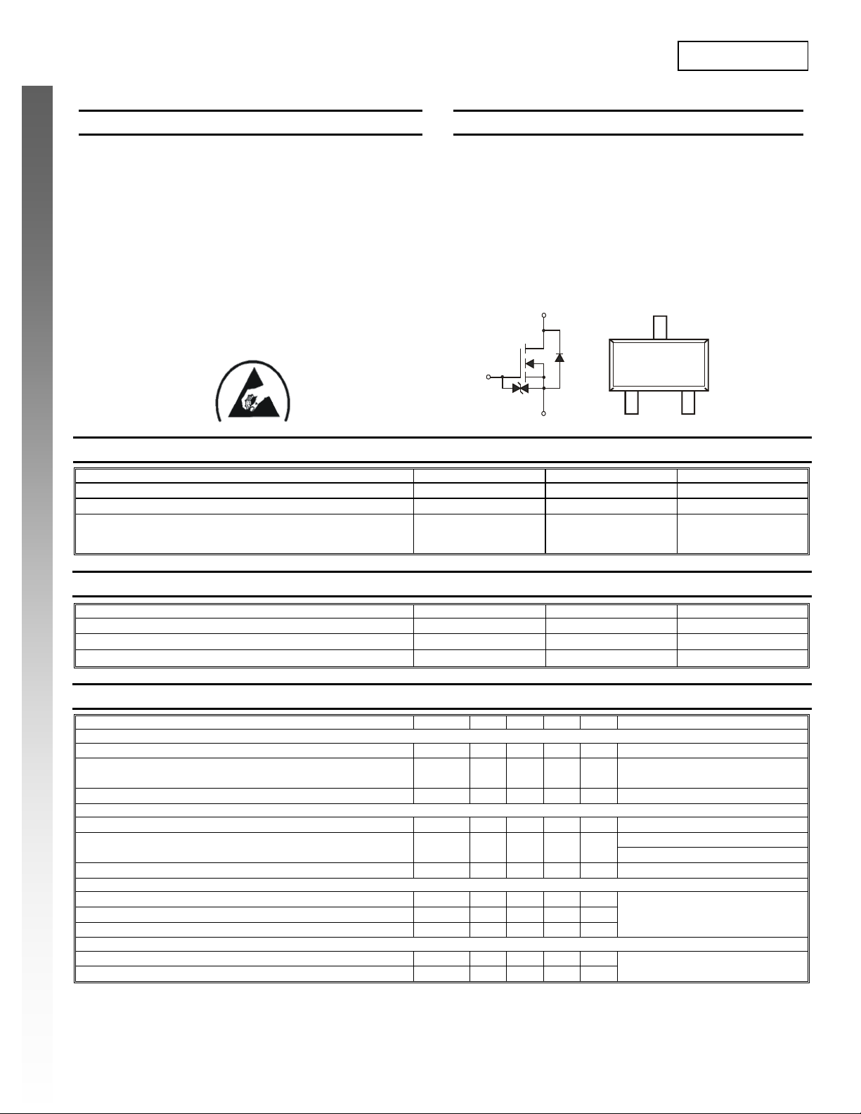
TOP VIEW
DMN66D0LT
N-CHANNEL ENHANCEMENT MODE MOSFET
Mechanical Data
• Case: SOT-523
• Case Material: Molded Plastic. UL Flammability Classification
Rating 94V-0
• Moisture Sensitivity: Level 1 per J-STD-020D
• Terminals: Solderable per MIL-STD-202, Method 208
• Lead Free Plating (Matte Tin Finish annealed over Alloy 42
leadframe).
• Terminal Connections: See Diagram
• Marking Information: See Page 3
• Ordering Information: See Page 3
• Weight: 0.002 grams (approximate)
SOT-523
Gate
V
DSS
V
GSS
I
D
Drain
Gate
Protection
Diode
EQUIVALENT CIRCUIT
Source
D
G
TOP VIEW
S
60 V
±20 V
115
73
800
mA
Thermal Characteristics @T
= 25°C unless otherwise specified
A
Characteristic Symbol Value Units
Total Power Dissipation
Thermal Resistance, Junction to Ambient
Operating and Storage Temperature Range
Electrical Characteristics @T
= 25°C unless otherwise specified
A
Characteristic Symbol Min Typ Max Unit Test Condition
OFF CHARACTERISTICS (Note 3)
Drain-Source Breakdown Voltage
Zero Gate Voltage Drain Current @ TC = 25°C
Gate-Body Leakage
ON CHARACTERISTICS (Note 3)
Gate Threshold Voltage
Forward Transconductance
DYNAMIC CHARACTERISTICS
Input Capacitance
Output Capacitance
Reverse Transfer Capacitance
SWITCHING CHARACTERISTICS
Turn-On Delay Time
Turn-Off Delay Time
Notes: 1. Device mounted on FR-4 PCB, 1 inch x 0.85 inch x 0.062 inch; pad layout as shown on Diodes Inc. suggested pad layout document AP02001, which
3. Short duration pulse test used to minimize self-heating effect.
can be found on our website at http://www.diodes.com/datasheets/ap02001.pdf.
2. No purposefully added lead.
DMN66D0LT
Document number: DS31530 Rev. 2 - 2
@ TC = 125°C
@ TJ = 125°C
P
D
R
JA
θ
T
J, TSTG
BV
DSS
⎯ ⎯
I
DSS
I
⎯ ⎯
GSS
V
GS(th)
R
⎯
DS (ON)
g
FS
C
⎯
iss
C
⎯
oss
C
⎯
rss
t
⎯
D(ON)
t
⎯
D(OFF)
1.2
1 of 4
www.diodes.com
60 70
⎯
3.5
3.0 6 5
80
⎯ ⎯
23
3.4
1.4
10
33
200 mW
625 °C/W
-55 to +150 °C
V
⎯
1.0
500
±5
2.0 V
⎯
⎯
⎯
⎯
⎯
µA
μA
Ω
mS
pF
pF
pF
ns
ns
V
= 0V, ID = 10μA
GS
V
= 60V, V
DS
±20V, V
V
GS =
V
= VGS, ID = 250μA
DS
V
= 5.0V, ID = 0.115A Static Drain-Source On-Resistance @ TJ = 25°C
GS
V
= 10V, ID = 0.115A
GS
V
= 10V, ID = 0.115A
DS
V
= 25V, VGS = 0V, f = 1.0MHz
DS
V
= 30V, ID = 0.115A, RL = 150Ω,
DD
= 10V, R
V
GEN
GS
DS
GEN
= 0V
= 0V
= 25Ω
September 2008
© Diodes Incorporated
Page 2
R
CUR
RENT
C, C
PACITANC
F
NEW PRODUCT
DMN66D0LT
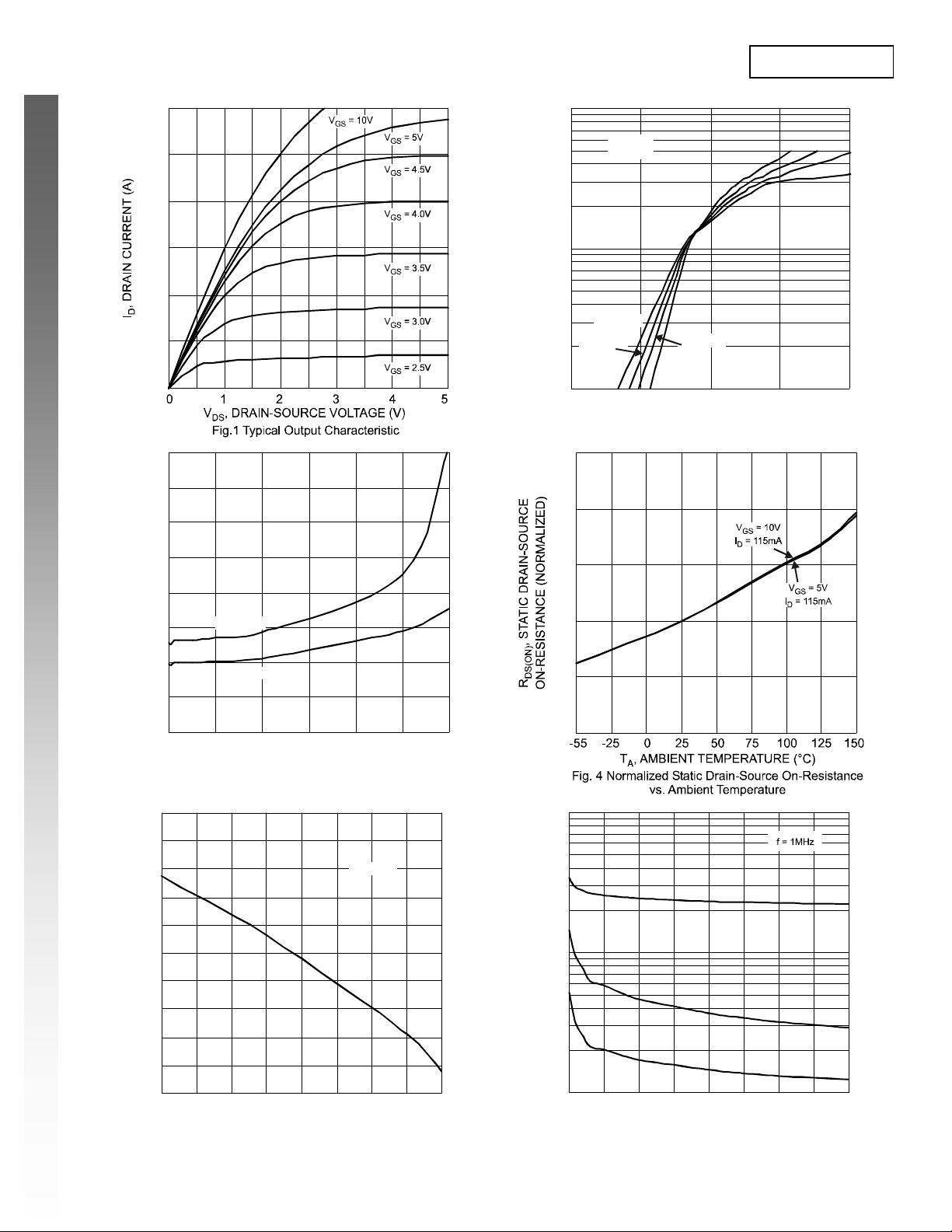
0.6
0.5
0.4
0.3
0.2
0.1
0
9
1
V = 5V
DS
Pulsed
(A)
0.1
AIN
D
I, D
0.01
T = 150°C
A
T = 85°C
A
T = 25°C
A
T = -55°C
A
1234
V , GATE SOURCE VOLTAGE (V)
GS
Fig. 2 Typical Transfer Characteristics
2.5
5
8
2.0
7
Ω
6
1.5
5
V = 5V
4
ON-RESISTANCE ( )
3
DS(ON)
R , STATIC DRAIN-SOURCE
2
GS
V = 10V
GS
1
0 0.1 0.2 0.3 0.4 0.5 0.6
I , DRAIN-SOURCE CURRENT (A)
D
Fig. 3 On-Resistance vs. Drain Current & Gate Voltage
2.0
1.9
1.8
I = 250µA
D
1.7
1.6
1.5
1.4
1.3
1.2
1.0
0.5
0
100
)
E (p
C
iss
10
A
T
C
oss
1.1
GS(TH)
V , GATE THRESHOLD VOLTAG E (V)
1.0
-50 -25 0 25 50 75 100 125 150
T , AMBIENT TEMPERATURE (°C)
Fig. 5 Gat e Threshold V ariation vs. Ambien t Temperature
A
1
0 5 10 15 20 25 30 35 40
V , DRAIN-SOURCE VOLTAGE (V)
DS
Fig. 6 Typical Total Capacitance
C
rss
DMN66D0LT
Document number: DS31530 Rev. 2 - 2
2 of 4
www.diodes.com
September 2008
© Diodes Incorporated
Page 3

OUR
CE CUR
RENT
DMN66D0LT
(A)
S
I, S
0.1
0.01
0.001
1
T = 150°C
A
T = 125°C
A
T = 85°C
A
T = 25°C
A
T = -55°C
A
0.0001
NEW PRODUCT
0.1 0.2 0.3 0.4 0.5 0.6 0.7 0.8 0.9 1
V , SOURCE-DRAIN VOLTAGE (V)
Fig. 7 Reverse Drain Current vs. Source-Drain Voltage
SD
Ordering Information (Note 4)
Part Number Case Packaging
DMN66D0LT-7 SOT-523 3000/Tape & Reel
Notes: 4. For packaging details, go to our website at http://www.diodes.com/datasheets/ap02007.pdf.
Marking Information
MN1
MN1 = Product Type Marking Code
YM = Date Code Marking
Y = Year ex: V = 2008
YM
M = Month ex: 9 = September
Date Code Key
Year 2008 2009 2010 2011 2012 2013 2014 2015
Code V W X Y Z A B C
Month Jan Feb Mar Apr May Jun Jul Aug Sep Oct Nov Dec
Code 1 2 3 4 5 6 7 8 9 O N D
Package Outline Dimensions
DMN66D0LT
Document number: DS31530 Rev. 2 - 2
K
J
A
SOT-523
Dim Min Max Typ
C
B
B 0.75 0.85
C 1.45 1.75
A 0.15 0.30
D
⎯ ⎯
G
H
N
M
G 0.90 1.10
H 1.50 1.70
J 0.00 0.10
K 0.60 0.80
L 0.10 0.30
M 0.10 0.20
D
L
N 0.45 0.65 0.50
0° 8°
0.22
0.80
1.60
0.50
1.00
1.60
0.05
0.75
0.22
0.12
⎯ α
All Dimensions in mm
3 of 4
www.diodes.com
September 2008
© Diodes Incorporated
Page 4

DMN66D0LT
Suggested Pad Layout
Diodes Incorporated and its subsidiaries reserve the right to make modifications, enhancements, improvements, corrections or other changes
without further notice to any product herein. Diodes Incorporated does not assume any liability arising out of the application or use of any product
NEW PRODUCT
described herein; neither does it convey any license under its patent rights, nor the rights of others. The user of products in such applications shall
assume all risks of such use and will agree to hold Diodes Incorporated and all the companies whose products are represented on our website,
harmless against all damages.
Diodes Incorporated products are not authorized for use as critical components in life support devices or systems without the expressed written
approval of the President of Diodes Incorporated.
Y
Z
X E
C
IMPORTANT NOTICE
LIFE SUPPORT
Dimensions Value (in mm)
Z 1.8
X 0.4
Y 0.51
C 1.3
E 0.7
DMN66D0LT
Document number: DS31530 Rev. 2 - 2
4 of 4
www.diodes.com
September 2008
© Diodes Incorporated
 Loading...